Global Gan Epitaxial Wafers Market
市场规模(十亿美元)
CAGR :
% 
 USD
1.20 Billion
USD
5.30 Billion
2024
2032
USD
1.20 Billion
USD
5.30 Billion
2024
2032
| 2025 –2032 | |
| USD 1.20 Billion | |
| USD 5.30 Billion | |
| % | |
全球 GAN 外延晶圓市場細分,按產品類型(GaN 同質外延晶圓、GaN 異質外延晶圓)、晶圓尺寸(2 英寸、4 英寸、6 英寸、8 英寸)、應用(光電器件、電力電子、高電子遷移率電晶體、電子圖像傳感器和射頻器件)、最終用戶(光電器件、電力電子、高電子遷移率電晶體、電力感測器和射頻器件)、最終用戶(電信、電信、電信
GAN外延晶圓市場分析
由於電力電子、光電子和射頻電子等各種應用對高性能半導體材料的需求不斷增加,GAN外延片市場取得了快速發展。 GAN(氮化鎵)外延片因其優異的導熱性、高擊穿電壓和高頻效率而廣受認可,使其成為功率元件、LED 和射頻組件的理想選擇。這導致 GAN 晶圓在電動車 (EV)、再生能源系統、5G 通訊基礎設施和 LED 照明等應用中迅速應用。各行業對小型化和功率效率的日益追求也推動了對 GAN 外延片的需求。
GAN外延片市場最重要的發展之一是晶圓生長技術的持續改進,包括MOCVD(金屬有機化學氣相沉積)和HVPE(氫化物氣相外延),從而可以生產出更高品質、缺陷更少的晶圓。這些創新使得 GAN 晶圓更具成本效益,並且適用於更廣泛的應用。
GAN外延晶圓市場規模
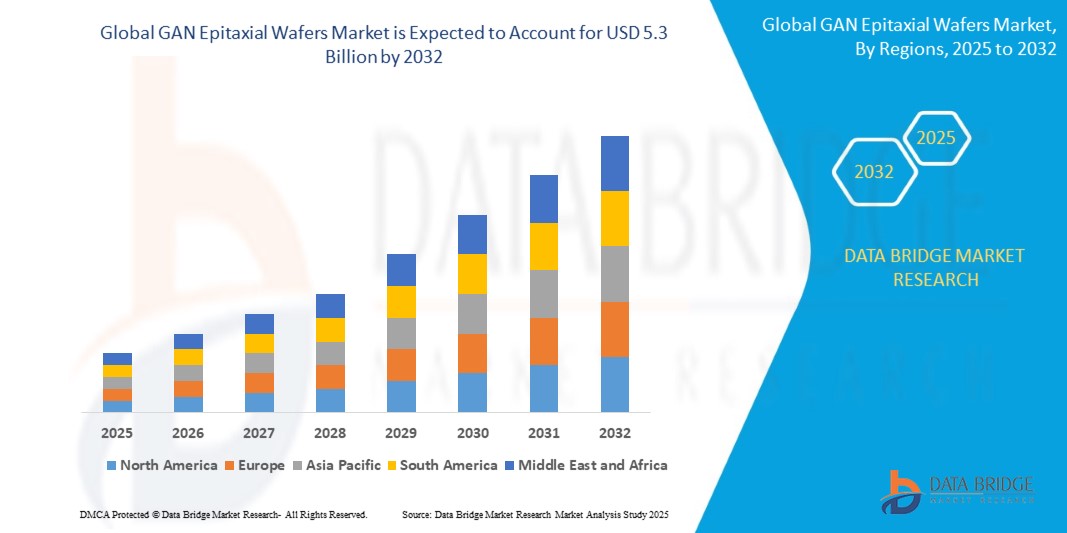
2024 年全球 GAN 外延片市場規模為 12 億美元,預計到 2032 年將達到 53 億美元,2025 年至 2032 年預測期間的複合年增長率為 20.60%。除了對市場價值、成長率、細分、地理覆蓋範圍和主要參與者等市場情景的洞察外,Data Bridge Market Research 策劃的市場報告還包括深入的專家分析、按地理位置代表的公司生產和產能、分銷商和合作夥伴的網絡佈局、詳細和更新的價格趨勢分析以及供應鏈和需求的缺口分析
GAN外延晶圓市場趨勢
“電力電子與5G應用的成長”
推動GAN外延晶圓市場成長的一個重要趨勢是對電動車(EV)和再生能源系統的需求不斷增長。 GaN 在高壓下的卓越功率轉換效率使其非常適合用於電動車充電器和太陽能逆變器等電力電子設備。例如,特斯拉等公司正在利用基於 GaN 的功率電晶體來提高其電動車充電系統的性能,從而縮短充電時間並提高效率。在再生能源領域,SolarEdge正在太陽能逆變器中使用 GaN 技術來提高能源轉換效率,促進太陽能的廣泛應用。此外,5G 網路的推出對 GaN 材料產生了巨大的需求,因為基於 GaN 的半導體可以在更高的頻率下工作,並為 5G 基地台和行動裝置提供更好的性能。高通和Qorvo等公司 正在將GaN技術整合到其5G射頻功率放大器中,以確保更快、更可靠的連接,並促進5G網路的全球部署。這一趨勢推動了對 GaN 外延片的需求,這對於提高電力電子和 5G 基礎設施的效率、小型化和性能至關重要。
報告範圍和GAN 外延晶圓市場細分
|
屬性 |
GAN外延晶圓關鍵市場洞察 |
|
涵蓋的領域 |
|
|
覆蓋國家 |
北美洲的美國、加拿大和墨西哥、德國、法國、英國、荷蘭、瑞士、比利時、俄羅斯、義大利、西班牙、土耳其、歐洲其他地區、中國、日本、印度、韓國、新加坡、馬來西亞、澳洲、泰國、印尼、菲律賓、亞太地區 (APAC) 的其他地區、沙烏地阿拉伯、阿聯酋、南非、埃及、以色列、中東和非洲 (MEA) 的其他地區、其他地區的歐洲地區 |
|
主要市場參與者 |
羅姆半導體(日本)、氮化鎵系統(加拿大)、日月光集團(台灣)、晶元光電股份有限公司(台灣)、英飛凌科技(德國)、Allegro MicroSystems(美國)、Qorvo(美國)、東京電子(日本)、日亞化學株式會社(日本)、聯合碳化矽(美國)、Cree(美國)、索尼株式會社(日本)、三菱電機(日本)、恩智浦半導體(荷蘭)、英飛科技(德國)、東芝株式會社(日本) Conversion Corporation(美國)、義法半導體(瑞士/法國)、Navitas Semiconductor Corporation(美國) |
|
市場機會 |
|
|
加值資料資訊集 |
除了對市場價值、成長率、細分、地理覆蓋範圍和主要參與者等市場情景的洞察之外,Data Bridge Market Research 策劃的市場報告還包括深入的專家分析、按地理位置表示的公司生產和產能、分銷商和合作夥伴的網絡佈局、詳細和更新的價格趨勢分析以及供應鏈和需求的缺口分析。 |
GAN外延晶圓市場定義
GaN(氮化鎵)外延片是用於製造高性能元件的半導體材料。它們是透過一種稱為外延的精確工藝生產的,其中在基底晶片上生長一層薄薄的 GaN。這些晶圓對於電力電子、高頻應用、光電子和通訊至關重要。 GaN 的寬頻隙和高電子遷移率使其成為 5G、LED 和電動車等高效、高功率應用的理想選擇。
GAN外延晶圓市場動態
驅動程式
- 對高性能功率元件的需求
電動車 (EV) 和太陽能等再生能源的日益普及,極大地推動了對 GaN 外延晶片的需求。 GaN 在功率轉換方面的卓越效率使其成為電動車中使用的逆變器和充電器等高性能功率設備的理想材料。隨著全球向永續能源解決方案轉變的不斷加強,基於 GaN 的元件對於提高電力電子能源效率變得越來越重要。 GaN 卓越的開關能力可減少能量損失並延長功率元件的使用壽命,進一步促進其在電動車領域和包括太陽能逆變器在內的再生能源應用領域的需求不斷增長。預計這一趨勢將支持GaN外延片市場的持續擴大。
- 5G基礎設施發展
5G網路的全球部署是GaN外延片市場的另一個關鍵驅動力。隨著對更快、更可靠的無線通訊系統的需求,基於 GaN 的射頻元件由於其能夠在更高的頻率下運行並且與矽等傳統材料相比具有更高的功率效率而獲得了顯著的吸引力。 GaN優異的熱導率和高擊穿電壓使其成為5G基地台和行動裝置中功率放大器和其他射頻組件的理想選擇。隨著全球對5G基礎設施的需求不斷擴大,GaN外延片正成為下一代無線通訊技術的關鍵推動者,從而推動市場成長。 GaN 在 5G 應用中提供的增強性能、能源效率和可靠性的組合將推動其在整個電信行業的應用。
機會
- 融入5G網絡
GaN外延片對於5G基礎設施的高效運作至關重要,它能夠在高頻下運作並在射頻組件中提供卓越的性能。隨著5G網路在全球持續推廣,GaN晶圓的需求預計將呈指數級增長。人們越來越依賴 5G 技術來實現更快的資料傳輸速度、增強的連接性和提高的網路可靠性,這為 GaN 外延片整合到基地台、行動裝置和網路基礎設施等廣泛應用中提供了巨大的機會。這種整合將在實現5G技術的先進功能方面發揮關鍵作用,為GaN晶圓製造商提供有希望的成長途徑。
- 晶圓生產的進步
GaN晶片生產的技術進步,例如金屬有機化學氣相沉積(MOCVD)和氫化物氣相外延(HVPE)技術,正在為市場帶來新的機會。這些創新提高了晶圓品質、改善了晶體結構並降低了生產成本,從而提高了 GaN 在更廣泛應用範圍內的經濟性和可及性。 GaN 生產製程的產量和可擴展性的提高有望推動其在電信、電力電子和再生能源等各個領域的應用。製造技術的持續進步也將為下一代GaN裝置的商業化鋪平道路,進一步推動市場的成長。
限制/挑戰
- 製造成本高
One of the significant challenges facing the GaN epitaxial wafers market is the high cost of manufacturing. The complex production processes, including the use of specialized equipment and high-quality raw materials, contribute to the elevated cost of GaN wafers. This factor can limit their adoption in cost-sensitive applications and industries, where budget constraints may favor alternative materials like silicon. While GaN offers superior performance in terms of power efficiency and thermal conductivity, the high initial cost of GaN wafers can present a barrier to widespread adoption, particularly in emerging markets or sectors with tight budgets. As such, reducing production costs remains a key challenge for manufacturers seeking to expand the market for GaN-based technologies.
- Supply Chain Constraints
The GaN epitaxial wafers market is also hindered by supply chain constraints, which can affect the availability and timely delivery of GaN wafers. With the increasing demand for GaN wafers in sectors such as telecommunications, automotive, and renewable energy, the limited number of suppliers and the high demand for these materials can lead to supply shortages or delays. These supply chain disruptions can result in higher prices and extended lead times, ultimately affecting market growth. Manufacturers and end-users must contend with these challenges, which could delay the widespread adoption of GaN technologies, especially in industries that rely on a constant and stable supply of high-quality wafers.
This market report provides details of new recent developments, trade regulations, import-export analysis, production analysis, value chain optimization, market share, impact of domestic and localized market players, analyses opportunities in terms of emerging revenue pockets, changes in market regulations, strategic market growth analysis, market size, category market growths, application niches and dominance, product approvals, product launches, geographic expansions, technological innovations in the market. To gain more info on the market contact Data Bridge Market Research for an Analyst Brief, our team will help you take an informed market decision to achieve market growth.
GAN Epitaxial Wafers Market Scope
The market is segmented on the basis of product type, Wafers size, application and end user. The growth amongst these segments will help you analyse meagre growth segments in the industries and provide the users with a valuable market overview and market insights to help them make strategic decisions for identifying core market applications.
Product Type
- GaN Homoepitaxial Epitaxial Wafer
- GaN Heteroepitaxial Epitaxial Wafer
Wafer Size
- 2 Inches
- 4 Inches
- 6 Inches
- 8 Inches
Application
- Optoelectronic Devices
- Power Electronics
- High Electron Mobility Transistors
- Radio Frequency Devices
- Image Sensors
End User
- Telecommunications
- Lighting & Displays
- Power Electronics
- Automotive
- Aerospace & Defense
GAN Epitaxial Wafers Market Regional Analysis
The market is analysed and market size insights and trends are provided by country, product type, Wafers size, application and end user as referenced above.
The countries covered in the market report are U.S., Canada and Mexico in North America, Germany, France, U.K., Netherlands, Switzerland, Belgium, Russia, Italy, Spain, Turkey, Rest of Europe in Europe, China, Japan, India, South Korea, Singapore, Malaysia, Australia, Thailand, Indonesia, Philippines, Rest of Asia-Pacific (APAC) in the Asia-Pacific (APAC), Saudi Arabia, U.A.E, South Africa, Egypt, Israel, Rest of Middle East and Africa (MEA) as a part of Middle East and Africa (MEA), Brazil, Argentina and Rest of South America as part of South America
Asia-Pacific is expected to dominate the GaN epitaxial wafers market due to the increasing adoption of GaN technology in key industries such as telecommunications, automotive, and renewable energy. The region benefits from rapid technological advancements, large-scale manufacturing capabilities, and government initiatives to support semiconductor development. In addition, the growing demand for 5G infrastructure and electric vehicles in countries like China, Japan, and South Korea contributes to the market's growth. The presence of leading manufacturers and a strong supply chain further reinforce Asia-Pacific's dominance in the market.
North America is expected to exhibit the highest growth rate in the GaN epitaxial wafers market during the forecast period due to increasing investments in research and development, especially in power electronics, 5G infrastructure, and renewable energy technologies. The region benefits from strong government initiatives, technological advancements, and a robust semiconductor industry. In addition, the presence of key market players and continuous advancements in GaN-based devices drive the demand for GaN epitaxial wafers, contributing to North America's rapid market growth.
The country section of the report also provides individual market impacting factors and changes in regulation in the market domestically that impacts the current and future trends of the market. Data points such as down-stream and upstream value chain analysis, technical trends and porter's five forces analysis, case studies are some of the pointers used to forecast the market scenario for individual countries. Also, the presence and availability of global brands and their challenges faced due to large or scarce competition from local and domestic brands, impact of domestic tariffs and trade routes are considered while providing forecast analysis of the country data.
GAN Epitaxial Wafers Market Share
市場競爭格局提供了競爭對手的詳細資訊。詳細資訊包括公司概況、公司財務狀況、收入、市場潛力、研發投資、新市場計劃、全球影響力、生產基地和設施、生產能力、公司優勢和劣勢、產品發布、產品寬度和廣度、應用優勢。以上提供的數據點僅與公司對市場的關注有關。
GAN 外延晶圓市場領導者包括:
- 羅姆半導體(日本)
- GaN Systems(加拿大)
- 日月光集團(台灣)
- 晶元光電股份有限公司 (中國台灣)
- 英飛凌科技(德國)
- Allegro MicroSystems(美國)
- Qorvo(美國)
- 東京電子(日本)
- 日亞化學株式會社(日本)
- 聯合碳化矽(美國)
- 克里語(美國)
- 索尼公司(日本)
- 三菱電機(日本)
- 恩智浦半導體(荷蘭)
- 英飛凌科技(德國)
- 東芝公司(日本)
- 松下公司(日本)
- NexGen Power Systems(美國)
- 高效率電源轉換公司(美國)
- 意法半導體(瑞士/法國)
- 納維半導體公司(美國)
GAN外延晶圓市場的最新發展
- 2024年11月,住友化學加速開發用於電力電子的大直徑GaN-on-GaN晶圓的專案被NEDO選定為2024財政年度專案。該計畫旨在推進六吋GaN-on-GaN晶圓的量產技術,瞄準電力基礎設施、資料中心和電動車等領域的節能電力電子應用。
- 2024年9月,英飛凌科技股份公司成功開發出全球首個300毫米功率氮化鎵(GaN)晶圓技術,使每片晶圓的晶片產量比200毫米晶圓高出2.3倍。這項突破顯著提高了效率並降低了成本,促進了 GaN 在汽車、消費電子和通訊等行業的廣泛應用。儘管面臨 GaN 與矽之間的應力和晶格失配等挑戰,英飛凌仍利用創新解決方案,特別是在其 GaN EPI 能力中心,將 GaN 技術擴展到大批量生產
- 2024年8月,MassPhoton Ltd與香港科技園區公司(HKSTP)合作,在InnoPark推出香港首條GaN外延晶圓試驗線。該項目投資 2 億港元,旨在推動該地區半導體產業發展並創造 250 多個就業機會
- 2024 年 8 月,SweGaN AB 報告稱,2024 年上半年碳化矽上氮化鎵 (GaN-on-SiC) 外延晶片的訂單為 1,700 萬瑞典克朗,成長 100%。該公司獲得了重要的電信和國防協議,從新工廠開始交付,並成功完成了 QuanFINE 外延片的客戶認證
- 2022年1月,總部位於韓國的IVWorks Co Ltd收購了法國材料公司聖戈班的GaN晶圓業務。此次收購增強了 IVWorks 量產用於功率元件的 4 吋至 12 吋 GaN 外延片的能力,包括電動車動力系統和防禦雷達的應用
SKU-
研究方法
数据收集和基准年分析是使用具有大样本量的数据收集模块完成的。该阶段包括通过各种来源和策略获取市场信息或相关数据。它包括提前检查和规划从过去获得的所有数据。它同样包括检查不同信息源中出现的信息不一致。使用市场统计和连贯模型分析和估计市场数据。此外,市场份额分析和关键趋势分析是市场报告中的主要成功因素。要了解更多信息,请请求分析师致电或下拉您的询问。
DBMR 研究团队使用的关键研究方法是数据三角测量,其中包括数据挖掘、数据变量对市场影响的分析和主要(行业专家)验证。数据模型包括供应商定位网格、市场时间线分析、市场概览和指南、公司定位网格、专利分析、定价分析、公司市场份额分析、测量标准、全球与区域和供应商份额分析。要了解有关研究方法的更多信息,请向我们的行业专家咨询。
可定制
Data Bridge Market Research 是高级形成性研究领域的领导者。我们为向现有和新客户提供符合其目标的数据和分析而感到自豪。报告可定制,包括目标品牌的价格趋势分析、了解其他国家的市场(索取国家列表)、临床试验结果数据、文献综述、翻新市场和产品基础分析。目标竞争对手的市场分析可以从基于技术的分析到市场组合策略进行分析。我们可以按照您所需的格式和数据样式添加您需要的任意数量的竞争对手数据。我们的分析师团队还可以为您提供原始 Excel 文件数据透视表(事实手册)中的数据,或者可以帮助您根据报告中的数据集创建演示文稿。

