
Global Gan Epitaxial Wafers Market
Market Size in USD Billion
 USD
1.20 Billion
USD
5.30 Billion
2024
2032
USD
1.20 Billion
USD
5.30 Billion
2024
2032
| 2025 - 2032 | |
| USD 1.20 Billion | |
| USD 5.30 Billion | |
| % | |
GAN Epitaxial Wafers Market Analysis
The GAN epitaxial wafers market has seen rapid advancements due to the increasing demand for high-performance semiconductor materials in various applications such as power electronics, optoelectronics, and RF electronics. GAN (Gallium Nitride) epitaxial wafers are widely recognized for their superior thermal conductivity, high breakdown voltage, and efficiency at high frequencies, making them ideal for use in power devices, LEDs, and RF components. This has led to the rapid adoption of GAN wafers in applications like electric vehicles (EVs), renewable energy systems, 5G communication infrastructure, and LED lighting. The growing trend toward miniaturization and power efficiency across industries is also propelling the demand for GAN epitaxial wafers.
One of the most significant developments in the GAN epitaxial wafer market is the continuous improvements in wafer growth techniques, including MOCVD (Metal-Organic Chemical Vapor Deposition) and HVPE (Hydride Vapor Phase Epitaxy), which have led to the production of higher-quality wafers with fewer defects. These innovations have made GAN wafers more cost-effective and accessible for a broader range of applications.
GAN Epitaxial Wafers Market Size
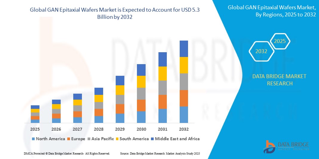
The global GAN epitaxial wafers market size was valued at USD 1.2 billion in 2024 and is projected to reach USD 5.3 billion by 2032, with a CAGR of 20.60% during the forecast period of 2025 to 2032. In addition to the insights on market scenarios such as market value, growth rate, segmentation, geographical coverage, and major players, the market reports curated by the Data Bridge Market Research also include in-depth expert analysis, geographically represented company-wise production and capacity, network layouts of distributors and partners, detailed and updated price trend analysis and deficit analysis of supply chain and demand
GAN Epitaxial Wafers Market Trends
“Growth in Power Electronics and 5G Applications”
One significant trend driving growth in the GAN epitaxial wafers market is the increasing demand for electric vehicles (EVs) and renewable energy systems. GaN’s superior power conversion efficiency at high voltages makes it ideal for use in power electronics such as EV chargers and solar inverters. For example, companies like Tesla are utilizing GaN-based power transistors to improve the performance of their EV charging systems, resulting in faster charging times and increased efficiency. In the renewable energy sector, SolarEdge is using GaN technology in solar inverters to boost energy conversion efficiency, contributing to the growing adoption of solar energy. Additionally, the rollout of 5G networks is creating significant demand for GaN materials, as GaN-based semiconductors can operate at higher frequencies and offer improved performance for 5G base stations and mobile devices. Companies like Qualcomm and Qorvo are integrating GaN technology in their 5G RF power amplifiers, ensuring faster, more reliable connections and facilitating the global deployment of 5G networks. This trend is fueling the demand for GaN epitaxial wafers, which are essential for enhancing the efficiency, miniaturization, and performance of power electronics and 5G infrastructure.
Report Scope and GAN Epitaxial Wafers Market Segmentation
|
Attributes |
GAN Epitaxial Wafers Key Market Insights |
|
Segments Covered |
|
|
Countries Covered |
U.S., Canada and Mexico in North America, Germany, France, U.K., Netherlands, Switzerland, Belgium, Russia, Italy, Spain, Turkey, Rest of Europe in Europe, China, Japan, India, South Korea, Singapore, Malaysia, Australia, Thailand, Indonesia, Philippines, Rest of Asia-Pacific (APAC) in the Asia-Pacific (APAC), Saudi Arabia, U.A.E., South Africa, Egypt, Israel, Rest of Middle East and Africa (MEA) as a part of Middle East and Africa (MEA), Brazil, Argentina and Rest of South America as part of South America |
|
Key Market Players |
Rohm Semiconductor (Japan), GaN Systems (Canada), ASE Group (Taiwan), Epistar Corporation (Taiwan), Infineon Technologies (Germany), Allegro MicroSystems (U.S.), Qorvo (U.S.), Tokyo Electron (Japan), Nichia Corporation (Japan), United Silicon Carbide (U.S.), Cree (U.S.), Sony Corporation (Japan), Mitsubishi Electric (Japan), NXP Semiconductors (Netherlands), Infineon Technologies (Germany), Toshiba Corporation (Japan), Panasonic Corporation (Japan), NexGen Power Systems (U.S.), Efficient Power Conversion Corporation (U.S.), STMicroelectronics (Switzerland/France), Navitas Semiconductor Corporation (U.S.) |
|
Market Opportunities |
|
|
Value Added Data Infosets |
In addition to the insights on market scenarios such as market value, growth rate, segmentation, geographical coverage, and major players, the market reports curated by the Data Bridge Market Research also include in-depth expert analysis, geographically represented company-wise production and capacity, network layouts of distributors and partners, detailed and updated price trend analysis and deficit analysis of supply chain and demand. |
GAN Epitaxial Wafers Market Definition
GaN (Gallium Nitride) epitaxial wafers are semiconductor materials used to manufacture high-performance devices. They are produced through a precise process called epitaxy, where a thin layer of GaN is grown on a substrate wafer. These wafers are crucial for power electronics, high-frequency applications, optoelectronics, and communications. GaN's wide bandgap and high electron mobility make it ideal for high-efficiency, high-power applications like 5G, LEDs, and electric vehicles.
GAN Epitaxial Wafers Market Dynamics
Drivers
- Demand for High-Performance Power Devices
The increasing adoption of electric vehicles (EVs) and renewable energy sources, such as solar power, is significantly driving the demand for GaN epitaxial wafers. GaN's exceptional efficiency in power conversion makes it an ideal material for high-performance power devices like inverters and chargers used in electric vehicles. As the global shift towards sustainable energy solutions intensifies, GaN-based components are becoming integral in enhancing the energy efficiency of power electronics. The superior switching capabilities of GaN reduce energy loss and increase the lifespan of power devices, further contributing to its growing demand in the EV sector and renewable energy applications, including solar inverters. This trend is expected to support the continuous expansion of the GaN epitaxial wafers market.
- 5G Infrastructure Development
The global rollout of 5G networks is another key driver for the GaN epitaxial wafers market. With the need for faster, more reliable wireless communication systems, GaN-based RF components are gaining significant traction due to their ability to operate at higher frequencies and deliver greater power efficiency compared to traditional materials like silicon. GaN's superior thermal conductivity and high breakdown voltage make it an ideal choice for power amplifiers and other RF components in 5G base stations and mobile devices. As the demand for 5G infrastructure expands globally, GaN epitaxial wafers are becoming a crucial enabler of next-generation wireless communication technologies, thereby fueling market growth. The combination of enhanced performance, energy efficiency, and reliability offered by GaN in 5G applications is set to drive its adoption across the telecom industry.
Opportunities
- Integration into 5G Networks
GaN epitaxial wafers are essential for the efficient operation of 5G infrastructure, with their ability to perform at high frequencies and deliver superior performance in RF components. As 5G networks continue to roll out globally, the demand for GaN wafers is expected to grow exponentially. The increasing reliance on 5G technology for faster data transfer speeds, enhanced connectivity, and improved network reliability presents a substantial opportunity for GaN epitaxial wafers to be integrated into a wide range of applications, including base stations, mobile devices, and network infrastructure. This integration will play a pivotal role in enabling the advanced features of 5G technology, offering a promising growth avenue for GaN wafer manufacturers.
- Advancements in Wafer Production
Technological advancements in GaN wafer production, such as Metal-Organic Chemical Vapor Deposition (MOCVD) and Hydride Vapor Phase Epitaxy (HVPE) techniques, are unlocking new opportunities in the market. These innovations enable better wafer quality, improved crystal structures, and reduced production costs, which, in turn, enhance the affordability and accessibility of GaN for a wider range of applications. The improved yield and scalability of GaN production processes are expected to drive its adoption across diverse sectors, including telecommunications, power electronics, and renewable energy. The continued advancements in manufacturing technologies will also pave the way for the commercialization of next-generation GaN devices, further propelling the market's growth.
Restraints/Challenges
- High Manufacturing Costs
One of the significant challenges facing the GaN epitaxial wafers market is the high cost of manufacturing. The complex production processes, including the use of specialized equipment and high-quality raw materials, contribute to the elevated cost of GaN wafers. This factor can limit their adoption in cost-sensitive applications and industries, where budget constraints may favor alternative materials like silicon. While GaN offers superior performance in terms of power efficiency and thermal conductivity, the high initial cost of GaN wafers can present a barrier to widespread adoption, particularly in emerging markets or sectors with tight budgets. As such, reducing production costs remains a key challenge for manufacturers seeking to expand the market for GaN-based technologies.
- Supply Chain Constraints
The GaN epitaxial wafers market is also hindered by supply chain constraints, which can affect the availability and timely delivery of GaN wafers. With the increasing demand for GaN wafers in sectors such as telecommunications, automotive, and renewable energy, the limited number of suppliers and the high demand for these materials can lead to supply shortages or delays. These supply chain disruptions can result in higher prices and extended lead times, ultimately affecting market growth. Manufacturers and end-users must contend with these challenges, which could delay the widespread adoption of GaN technologies, especially in industries that rely on a constant and stable supply of high-quality wafers.
This market report provides details of new recent developments, trade regulations, import-export analysis, production analysis, value chain optimization, market share, impact of domestic and localized market players, analyses opportunities in terms of emerging revenue pockets, changes in market regulations, strategic market growth analysis, market size, category market growths, application niches and dominance, product approvals, product launches, geographic expansions, technological innovations in the market. To gain more info on the market contact Data Bridge Market Research for an Analyst Brief, our team will help you take an informed market decision to achieve market growth.
GAN Epitaxial Wafers Market Scope
The market is segmented on the basis of product type, Wafers size, application and end user. The growth amongst these segments will help you analyse meagre growth segments in the industries and provide the users with a valuable market overview and market insights to help them make strategic decisions for identifying core market applications.
Product Type
- GaN Homoepitaxial Epitaxial Wafer
- GaN Heteroepitaxial Epitaxial Wafer
Wafer Size
- 2 Inches
- 4 Inches
- 6 Inches
- 8 Inches
Application
- Optoelectronic Devices
- Power Electronics
- High Electron Mobility Transistors
- Radio Frequency Devices
- Image Sensors
End User
- Telecommunications
- Lighting & Displays
- Power Electronics
- Automotive
- Aerospace & Defense
GAN Epitaxial Wafers Market Regional Analysis
The market is analysed and market size insights and trends are provided by country, product type, Wafers size, application and end user as referenced above.
The countries covered in the market report are U.S., Canada and Mexico in North America, Germany, France, U.K., Netherlands, Switzerland, Belgium, Russia, Italy, Spain, Turkey, Rest of Europe in Europe, China, Japan, India, South Korea, Singapore, Malaysia, Australia, Thailand, Indonesia, Philippines, Rest of Asia-Pacific (APAC) in the Asia-Pacific (APAC), Saudi Arabia, U.A.E, South Africa, Egypt, Israel, Rest of Middle East and Africa (MEA) as a part of Middle East and Africa (MEA), Brazil, Argentina and Rest of South America as part of South America
Asia-Pacific is expected to dominate the GaN epitaxial wafers market due to the increasing adoption of GaN technology in key industries such as telecommunications, automotive, and renewable energy. The region benefits from rapid technological advancements, large-scale manufacturing capabilities, and government initiatives to support semiconductor development. In addition, the growing demand for 5G infrastructure and electric vehicles in countries like China, Japan, and South Korea contributes to the market's growth. The presence of leading manufacturers and a strong supply chain further reinforce Asia-Pacific's dominance in the market.
North America is expected to exhibit the highest growth rate in the GaN epitaxial wafers market during the forecast period due to increasing investments in research and development, especially in power electronics, 5G infrastructure, and renewable energy technologies. The region benefits from strong government initiatives, technological advancements, and a robust semiconductor industry. In addition, the presence of key market players and continuous advancements in GaN-based devices drive the demand for GaN epitaxial wafers, contributing to North America's rapid market growth.
The country section of the report also provides individual market impacting factors and changes in regulation in the market domestically that impacts the current and future trends of the market. Data points such as down-stream and upstream value chain analysis, technical trends and porter's five forces analysis, case studies are some of the pointers used to forecast the market scenario for individual countries. Also, the presence and availability of global brands and their challenges faced due to large or scarce competition from local and domestic brands, impact of domestic tariffs and trade routes are considered while providing forecast analysis of the country data.
GAN Epitaxial Wafers Market Share
The market competitive landscape provides details by competitor. Details included are company overview, company financials, revenue generated, market potential, investment in research and development, new market initiatives, global presence, production sites and facilities, production capacities, company strengths and weaknesses, product launch, product width and breadth, application dominance. The above data points provided are only related to the companies' focus related to market.
GAN Epitaxial Wafers Market Leaders Operating in the Market Are:
- Rohm Semiconductor (Japan)
- GaN Systems (Canada)
- ASE Group (Taiwan)
- Epistar Corporation (Taiwan)
- Infineon Technologies (Germany)
- Allegro MicroSystems (U.S.)
- Qorvo (U.S.)
- Tokyo Electron (Japan)
- Nichia Corporation (Japan)
- United Silicon Carbide (U.S.)
- Cree (U.S.)
- Sony Corporation (Japan)
- Mitsubishi Electric (Japan)
- NXP Semiconductors (Netherlands)
- Infineon Technologies (Germany)
- Toshiba Corporation (Japan)
- Panasonic Corporation (Japan)
- NexGen Power Systems (U.S.)
- Efficient Power Conversion Corporation (U.S.)
- STMicroelectronics (Switzerland/France)
- Navitas Semiconductor Corporation (U.S.)
Latest Developments in GAN Epitaxial Wafers Market
- In November 2024, Sumitomo Chemical's project to accelerate the development of large-diameter GaN-on-GaN wafers for power electronics has been selected by NEDO for FY 2024. The initiative aims to advance mass production technology for six-inch GaN-on-GaN wafers, targeting energy-efficient power electronics applications in sectors like electrical infrastructure, data centers, and electric vehicles
- In September 2024, Infineon Technologies AG has successfully developed the world’s first 300 mm power gallium nitride (GaN) wafer technology, enabling the production of 2.3 times more chips per wafer than 200 mm wafers. This breakthrough offers significant efficiency gains and cost reductions, facilitating the widespread adoption of GaN in industries like automotive, consumer electronics, and communications. Despite challenges such as stress and lattice mismatch between GaN and silicon, Infineon has leveraged innovative solutions, particularly at its Center of Competence for GaN EPI, to scale GaN technology for high-volume manufacturing
- In August 2024, MassPhoton Ltd, in collaboration with Hong Kong Science and Technology Parks Corporation (HKSTP), is launching Hong Kong's first GaN epitaxial wafer pilot line at InnoPark. This initiative, with a HK$200m investment, aims to advance the region's semiconductor industry and create over 250 jobs
- In August 2024, SweGaN AB reported 17 MSEK in orders for Gallium Nitride on Silicon Carbide (GaN-on-SiC) epitaxial wafers in H1 2024, marking a 100% increase. The company secured major telecom and defense agreements, launched deliveries from a new facility, and completed successful customer qualification for its QuanFINE epiwafers
- In January 2022, IVWorks Co Ltd, based in South Korea, has acquired the GaN wafer business from Saint-Gobain, a French materials company. The acquisition strengthens IVWorks' capabilities in mass-producing 4- to 12-inch GaN epiwafers for power devices, including applications in EV powertrains and defense radars
SKU-
- Interactive Data Analysis Dashboard
- Company Analysis Dashboard for high growth potential opportunities
- Research Analyst Access for customization & queries
- Competitor Analysis with Interactive dashboard
- Latest News, Updates & Trend analysis
- Harness the Power of Benchmark Analysis for Comprehensive Competitor Tracking
Global Gan Epitaxial Wafers Market, Supply Chain Analysis and Ecosystem Framework
To support market growth and help clients navigate the impact of geopolitical shifts, DBMR has integrated in-depth supply chain analysis into its Global Gan Epitaxial Wafers Market research reports. This addition empowers clients to respond effectively to global changes affecting their industries. The supply chain analysis section includes detailed insights such as Global Gan Epitaxial Wafers Market consumption and production by country, price trend analysis, the impact of tariffs and geopolitical developments, and import and export trends by country and HSN code. It also highlights major suppliers with data on production capacity and company profiles, as well as key importers and exporters. In addition to research, DBMR offers specialized supply chain consulting services backed by over a decade of experience, providing solutions like supplier discovery, supplier risk assessment, price trend analysis, impact evaluation of inflation and trade route changes, and comprehensive market trend analysis.
Data collection and base year analysis are done using data collection modules with large sample sizes. The stage includes obtaining market information or related data through various sources and strategies. It includes examining and planning all the data acquired from the past in advance. It likewise envelops the examination of information inconsistencies seen across different information sources. The market data is analysed and estimated using market statistical and coherent models. Also, market share analysis and key trend analysis are the major success factors in the market report. To know more, please request an analyst call or drop down your inquiry.
The key research methodology used by DBMR research team is data triangulation which involves data mining, analysis of the impact of data variables on the market and primary (industry expert) validation. Data models include Vendor Positioning Grid, Market Time Line Analysis, Market Overview and Guide, Company Positioning Grid, Patent Analysis, Pricing Analysis, Company Market Share Analysis, Standards of Measurement, Global versus Regional and Vendor Share Analysis. To know more about the research methodology, drop in an inquiry to speak to our industry experts.
Data Bridge Market Research is a leader in advanced formative research. We take pride in servicing our existing and new customers with data and analysis that match and suits their goal. The report can be customized to include price trend analysis of target brands understanding the market for additional countries (ask for the list of countries), clinical trial results data, literature review, refurbished market and product base analysis. Market analysis of target competitors can be analyzed from technology-based analysis to market portfolio strategies. We can add as many competitors that you require data about in the format and data style you are looking for. Our team of analysts can also provide you data in crude raw excel files pivot tables (Fact book) or can assist you in creating presentations from the data sets available in the report.


