O ALD é uma tecnologia de deposição de filme fino que permite um controlo preciso da espessura e composição do filme. Isto torna-o ideal para uma variedade de aplicações, tais como semicondutores, eletrónica, células solares, dispositivos médicos e sensores. O ALD é também uma tecnologia relativamente nova, o que significa que ainda há espaço para crescimento no mercado. Os métodos tradicionais de deposição de película fina, como o CVD, podem ser dispendiosos. O ALD é uma alternativa mais económica, o que está a impulsionar a sua adoção em diversos setores.
Aceda ao relatório completo em https://www.databridgemarketresearch.com/reports/global-atomic-layer-deposition-market
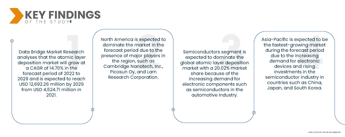
A Data Bridge Market Research analisa que o mercado de deposição de camada atómica crescerá a um CAGR de 14,70% no período previsto de 2022 a 2029 e deverá atingir os 12.692,26 milhões de dólares até 2029, face aos 4.524,71 milhões de dólares em 2021. A médio prazo, prevê-se que a crescente utilização de hélio nas indústrias de eletrónica e semicondutores e a crescente utilização no setor da saúde impulsionar a procura do mercado. Por outro lado, prevê-se que o elevado custo do procedimento de extracção e as rigorosas regras governamentais sobre a utilização do hélio dificultem o crescimento do mercado. Prevê-se que o desenvolvimento de sistemas eficientes de armazenamento e transporte de gás e as grandes reservas de gás natural descobertas na Tanzânia apresentem diversas oportunidades ao longo do período projectado.
A crescente procura por semicondutores e eletrónica deverá impulsionar a taxa de crescimento do mercado
Espera-se que o mercado global de semicondutores atinja 1 bilião de dólares até 2030. A crescente procura por dispositivos eletrónicos, como smartphones, tablets e computadores portáteis, impulsiona este crescimento. O ALD é uma tecnologia fundamental no fabrico de semicondutores, pois permite um controlo preciso da espessura e da composição do filme. O ALD pode ser utilizado para depositar uma variedade de materiais, incluindo metais, óxidos e nitretos. Estes materiais podem ser utilizados para criar filmes finos de alto desempenho para uma variedade de aplicações, tais como células solares, dispositivos médicos e sensores. A tendência para a miniaturização está a impulsionar a procura por ALD. O ALD é uma tecnologia essencial no fabrico de dispositivos pequenos e de alto desempenho, como transístores e circuitos integrados.
Âmbito do Relatório e Segmentação de Mercado
Métrica de Reporte
|
Detalhes
|
Período de previsão
|
2022 a 2029
|
Ano base
|
2021
|
Anos Históricos
|
2020 (personalizável para 2014-2019)
|
Unidades quantitativas
|
Receita em milhões de dólares americanos, volumes em unidades, preços em dólares americanos
|
Segmentos abrangidos
|
Tipo de produto (ALD de metal, ALD de óxido de alumínio, ALD melhorado por plasma, ALD catalítico, outros), aplicação (semicondutores, dispositivos solares, eletrónica, equipamento médico, instalações de investigação e desenvolvimento, células de combustível, dispositivos óticos, materiais termoelétricos, cabeças magnéticas, sensores, camadas de barreira, camadas de primer, aplicação não IC, outros)
|
Países abrangidos
|
EUA, Canadá e México na América do Norte, Alemanha, França, Reino Unido, Holanda, Suíça, Bélgica, Rússia, Itália, Espanha, Turquia, Resto da Europa na Europa, China, Japão, Índia, Coreia do Sul, Singapura, Malásia, Austrália, Tailândia, Indonésia, Filipinas, Resto da Ásia-Pacífico (APAC) na Ásia-Pacífico (APAC), Arábia Saudita, Emirados Árabes Unidos, África do Sul, Egito, Israel, Resto do Médio Oriente e África (MEA) como parte do Médio Oriente e África (MEA), Brasil, Argentina e Resto da América do Sul como parte da América do Sul
|
Participantes do mercado abrangidos
|
ADEKA CORPORATION (Japão), AIXTRON (Alemanha), Applied Materials Inc. (EUA), ASM International (EUA), LAM RESEARCH CORPORATION (EUA), Tokyo Electron Limited (Japão), Kurt J. Lesker Company (EUA), Beneq (Taiwan), Veeco Instruments Inc. (EUA), ANRIC TECH. (EUA), Encapsulix (França), SENTECH Instruments GmbH (Alemanha), Oxford Instruments (Reino Unido), Forge Nano Inc. (EUA), Merck KGaA (Alemanha), HZO, Inc. (EUA), Picosun Oy. (Finlândia)
|
Pontos de dados abordados no relatório
|
Para além dos insights sobre os cenários de mercado, tais como o valor de mercado, a taxa de crescimento, a segmentação, a cobertura geográfica e os principais participantes, os relatórios de mercado selecionados pela Data Bridge Market Research incluem também análises aprofundadas de especialistas, produção e capacidade das empresas representadas geograficamente, layouts de rede de distribuidores e parceiros, análise detalhada e atualizada das tendências de preços e análise do défice da cadeia de abastecimento e da procura.
|
Análise de Segmentos:
O mercado global de deposição de camadas atómicas está segmentado em dois segmentos notáveis com base no tipo de produto e aplicação.
- Com base no tipo de produto, o mercado global de deposição de camada atómica está segmentado em ALD de metal, ALD de óxido de alumínio, ALD melhorado por plasma, ALD catalítico e outros. Espera-se que o segmento de ALD metálico domine o mercado global de deposição de camada atómica com uma quota de mercado de 42,08% porque esta técnica de deposição de filme ultrafino encontrou muitas aplicações devido às suas capacidades distintas.
O segmento de ALD metálico dominará o segmento de tipos de produtos do mercado de deposição de camadas atómicas
O segmento de ALD de metal emergirá como o segmento dominante em termos de tipo de produto. Isto deve-se ao número crescente de atividades de desenvolvimento de infraestruturas no mercado, especialmente nas economias em desenvolvimento. Além disso, o crescimento e a expansão da indústria química a nível mundial impulsionarão ainda mais o crescimento deste segmento.
- Com base na aplicação, o mercado global de deposição de camadas atómicas está segmentado em semicondutores, dispositivos solares, eletrónica, equipamentos médicos, instalações de investigação e desenvolvimento, células de combustível, dispositivos óticos, materiais termoelétricos, cabeças magnéticas, sensores, camadas de barreira, camadas de primer, aplicações não IC e outros. Espera-se que o segmento de semicondutores domine o mercado global de deposição de camada atómica com uma quota de mercado de 20,02% devido à crescente procura de componentes eletrónicos, como semicondutores, na indústria automóvel.
O segmento dos semicondutores dominará o segmento de aplicação do mercado de deposição de camada atómica
O segmento dos semicondutores emergirá como o segmento de aplicação dominante. Isto deve-se ao número crescente de empresas de semicondutores no mercado, especialmente nas economias em desenvolvimento. Além disso, o crescimento e a expansão dos serviços de desenvolvimento de investigação à escala global impulsionarão ainda mais o crescimento deste segmento.
Principais jogadores
A Data Bridge Market Research reconhece as seguintes empresas como os principais participantes do mercado: ADEKA CORPORATION (Japão), AIXTRON (Alemanha), Applied Materials Inc. (EUA), ASM International (EUA), LAM RESEARCH CORPORATION (EUA), Tokyo Electron Limited (Japão), Kurt J. Lesker Company (EUA), Beneq (Taiwan), Veeco Instruments Inc. (EUA), ANRIC TECH. (EUA), Encapsulix (França), SENTECH Instruments GmbH (Alemanha), Oxford Instruments (Reino Unido), Forge Nano Inc. (EUA), Merck KGaA (Alemanha), HZO, Inc. (EUA), Picosun Oy (Finlândia).
Desenvolvimento de Mercado
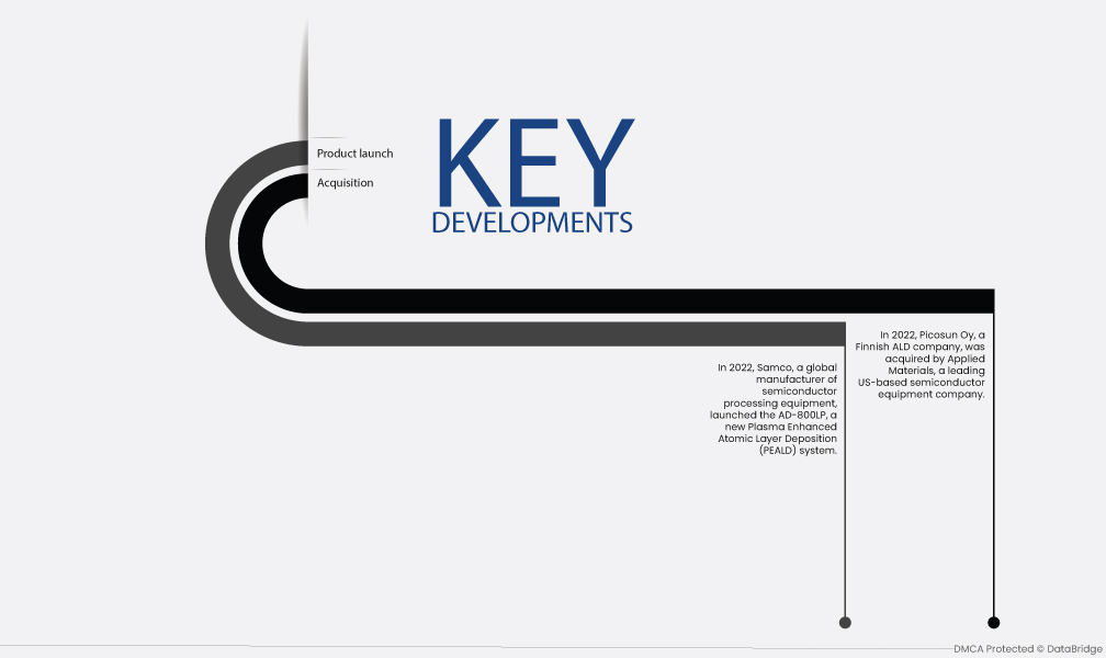
- Em 2022, a Samco, fabricante global de equipamentos de processamento de semicondutores, lançou o AD-800LP, um novo sistema de deposição de camada atómica melhorada por plasma (PEALD). O AD-800LP foi concebido para depositar filmes de óxido de porta para dispositivos de energia de última geração feitos de materiais de carboneto de silício (SiC) e nitreto de gálio (GaN). Estes materiais são essenciais para o desenvolvimento de tecnologias neutras em carbono.
- Em 2022, a Picosun Oy, uma empresa finlandesa de ALD, foi adquirida pela Applied Materials, uma empresa líder de equipamentos semicondutores com sede nos EUA. Esta aquisição foi a maior saída na história da CapMan, uma empresa de capital privado que investiu na Picosun em 2014. A Picosun é pioneira no campo da ALD, e as empresas líderes nos setores de semicondutores, eletrónica e energia solar utilizam a sua tecnologia.
Análise Regional
Geograficamente, os países abrangidos pelo relatório de mercado são os EUA, Canadá e México na América do Norte, Alemanha, França, Reino Unido, Holanda, Suíça, Bélgica, Rússia, Itália, Espanha, Turquia, Resto da Europa na Europa, China, Japão, Índia, Coreia do Sul, Singapura, Malásia, Austrália, Tailândia, Indonésia, Filipinas, Resto da Ásia-Pacífico (APAC) na Ásia-Pacífico (APAC), Arábia Saudita, Emirados Árabes Unidos, África do Sul, Egito, Israel, Resto do Médio Oriente e África (MEA) como parte do Médio Oriente e África (MEA), Brasil, Argentina e Resto da América do Sul como parte da América do Sul.
De acordo com a análise de pesquisa de mercado da Data Bridge:
A América do Norte é a região dominante no mercado de deposição de camadas atómicas durante o período previsto de 2022-2029
Espera-se que a América do Norte domine o mercado no período previsto devido aos principais participantes da região, como a Cambridge Nanotech, Inc., a Picosun Oy e a Lam Research Corporation. A região alberga também um grande número de empresas fabricantes de semicondutores, que estão a impulsionar a procura por sistemas de deposição de camada atómica (ALD).
Estima-se que a Ásia-Pacífico seja a região de crescimento mais rápido no mercado de deposição de camadas atómicas no período previsto de 2022-2029
Prevê-se que a Ásia-Pacífico seja o mercado de crescimento mais rápido durante o período previsto devido à crescente procura de dispositivos eletrónicos e ao aumento dos investimentos na indústria de semicondutores em países como a China, o Japão e a Coreia do Sul.
Para obter informações mais detalhadas sobre o relatório de mercado de deposição de camada atómica, clique aqui – https://www.databridgemarketresearch.com/reports/global-atomic-layer-deposition-market
