Global Semiconductor Packaging Market
Market Size in USD Billion
CAGR :
% 
 USD
42.60 Billion
USD
78.85 Billion
2025
2033
USD
42.60 Billion
USD
78.85 Billion
2025
2033
| 2026 –2033 | |
| USD 42.60 Billion | |
| USD 78.85 Billion | |
| % | |
|
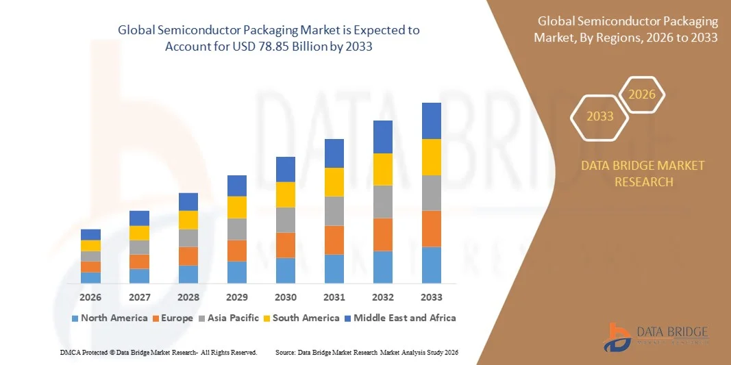
Semiconductor Packaging Market Size
- The global semiconductor packaging market size was valued at USD 42.60 billion in 2025 and is expected to reach USD 78.85 billion by 2033, at a CAGR of 8.00% during the forecast period
- The market growth is largely fuelled by rising demand for advanced integrated circuits across consumer electronics, automotive electronics, and industrial automation applications
- Increasing adoption of advanced packaging technologies such as flip chip, wafer-level packaging, and system-in-package to support higher performance and miniaturisation requirements
Semiconductor Packaging Market Analysis
- The market is witnessing steady transformation driven by the need for higher functionality, improved thermal management, and enhanced electrical performance in compact electronic devices
- Growing complexity of semiconductor designs is pushing manufacturers to invest in innovative packaging solutions that enable better power efficiency and signal integrity
- Asia-Pacific dominated the semiconductor packaging market with the largest revenue share in 2025, driven by the strong presence of semiconductor manufacturing hubs, high-volume electronics production, and continuous investments in advanced packaging technologies
- North America region is expected to witness the highest growth rate in the global semiconductor packaging market, driven by expanding local manufacturing capacity, increased R&D spending, and strong policy support aimed at strengthening the regional semiconductor value chain
- The Flip-Chip segment held the largest market revenue share in 2025 driven by its superior electrical performance, high I/O density, and efficient heat dissipation capabilities. Flip-Chip packaging is widely adopted in high-performance processors, GPUs, and advanced consumer electronics due to its ability to support miniaturisation and higher operating speeds
Report Scope and Semiconductor Packaging Market Segmentation
|
Attributes |
Semiconductor Packaging Key Market Insights |
|
Segments Covered |
|
|
Countries Covered |
North America
Europe
Asia-Pacific
Middle East and Africa
South America
|
|
Key Market Players |
|
|
Market Opportunities |
|
|
Value Added Data Infosets |
In addition to the insights on market scenarios such as market value, growth rate, segmentation, geographical coverage, and major players, the market reports curated by the Data Bridge Market Research also include import export analysis, production capacity overview, production consumption analysis, price trend analysis, climate change scenario, supply chain analysis, value chain analysis, raw material/consumables overview, vendor selection criteria, PESTLE Analysis, Porter Analysis, and regulatory framework. |
Semiconductor Packaging Market Trends
Rising Adoption of Advanced and Heterogeneous Packaging Technologies
- The increasing demand for high-performance, compact, and energy-efficient semiconductor devices is significantly shaping the semiconductor packaging market, as manufacturers focus on advanced packaging solutions that support higher I/O density, improved thermal performance, and enhanced electrical efficiency. Technologies such as flip chip, wafer-level packaging, fan-out packaging, and system-in-package are gaining traction due to their ability to meet miniaturisation and performance requirements without compromising reliability. This trend is strengthening adoption across consumer electronics, automotive, industrial, and data centre applications, encouraging continuous innovation in packaging design and materials
- Growing deployment of advanced computing applications, including artificial intelligence, high-performance computing, and 5G infrastructure, has accelerated the demand for sophisticated packaging solutions capable of handling higher power densities and faster data transmission. Semiconductor packaging is increasingly viewed as a critical enabler of overall device performance, leading to higher investment in R&D and closer collaboration between chip designers, foundries, and packaging service providers
- The shift toward heterogeneous integration is influencing purchasing and design decisions, with manufacturers emphasizing multi-die integration, improved interconnect technologies, and advanced substrates. These factors are helping companies differentiate products in a competitive semiconductor landscape while addressing performance, size, and cost challenges. Packaging innovations are also being highlighted in product launches and technology roadmaps to strengthen market positioning and customer confidence
- For instance, in 2024, Intel in the U.S. and TSMC in Taiwan expanded their advanced packaging capabilities through technologies such as chiplet-based architectures and 3D packaging solutions. These developments were introduced to support next-generation processors and high-performance applications, with adoption across data centres, AI accelerators, and advanced consumer devices. The initiatives also reinforced long-term partnerships with fabless semiconductor companies and system OEMs
- While demand for advanced semiconductor packaging continues to grow, sustained market expansion depends on balancing performance improvements with cost efficiency, yield optimisation, and scalability. Packaging providers are focusing on improving manufacturing throughput, material innovation, and automation to meet rising volume requirements while maintaining quality and reliability standards
Semiconductor Packaging Market Dynamics
Driver
Growing Demand for High-Performance and Miniaturised Semiconductor Devices
- Rising demand for high-performance computing, AI-enabled systems, and advanced consumer electronics is a major driver for the semiconductor packaging market. Manufacturers are increasingly adopting advanced packaging technologies to overcome limitations of traditional scaling, enhance performance, and reduce power consumption. This trend is also driving innovation in materials, interconnects, and thermal management solutions
- Expanding applications in smartphones, electric vehicles, data centres, and industrial automation are supporting market growth. Semiconductor packaging plays a critical role in enabling compact form factors, higher functionality, and improved durability, allowing device manufacturers to meet evolving performance and reliability expectations
- Semiconductor companies and OSAT providers are actively investing in capacity expansion, technology upgrades, and strategic partnerships to address rising demand. These efforts are supported by long-term technology roadmaps and co-development initiatives across the semiconductor value chain, helping accelerate time-to-market and improve overall system performance
- For instance, in 2023, Samsung Electronics in South Korea and ASE Technology in Taiwan reported increased investments in advanced packaging lines to support high-density memory and logic devices. These initiatives were driven by growing demand from AI servers, automotive electronics, and advanced consumer products, contributing to higher order volumes and stronger customer engagement
- Although strong demand fundamentals support market growth, long-term momentum will depend on continuous innovation, skilled workforce availability, and alignment between chip design and packaging technologies. Ongoing investment in automation, process control, and advanced testing will be critical to sustain competitiveness
Restraint/Challenge
High Capital Investment and Process Complexity
- The high capital expenditure required for advanced semiconductor packaging equipment and facilities remains a key challenge, particularly for smaller players. Advanced packaging processes involve complex manufacturing steps, stringent quality control, and expensive materials, which increase operational costs and limit rapid capacity expansion
- Technical complexity and yield management pose additional challenges, as advanced packaging requires precise alignment, bonding, and thermal control. Any defects in packaging can directly impact device performance and reliability, leading to higher scrap rates and increased production costs if not managed effectively
- Supply chain constraints and dependence on specialised materials and equipment also affect market growth. Limited availability of advanced substrates, bonding tools, and inspection systems can create bottlenecks, while long lead times add to cost pressures and production risks
- For instance, in 2024, packaging service providers supporting automotive and data centre customers in Japan and Germany reported delays and higher costs due to limited availability of advanced substrates and inspection equipment. These constraints affected delivery timelines and increased pricing pressure for end customers, influencing procurement decisions
- Addressing these challenges will require continuous investment in process optimisation, equipment innovation, and supply chain diversification. Collaboration between equipment suppliers, material providers, and packaging companies, along with standardisation efforts, will be essential to improve efficiency, reduce costs, and support long-term growth of the global semiconductor packaging market
Semiconductor Packaging Market Scope
The market is segmented on the basis of type, packaging material, wafer material, technology, and end user.
- By Type
On the basis of type, the semiconductor packaging market is segmented into Flip-Chip, Embedded Die, Fan-In WLP, and Fan-Out WLP. The Flip-Chip segment held the largest market revenue share in 2025 driven by its superior electrical performance, high I/O density, and efficient heat dissipation capabilities. Flip-Chip packaging is widely adopted in high-performance processors, GPUs, and advanced consumer electronics due to its ability to support miniaturisation and higher operating speeds.
The Fan-Out WLP segment is expected to witness the fastest growth rate from 2026 to 2033, driven by increasing demand for compact, high-density, and cost-efficient packaging solutions. Fan-Out WLP enables better performance, thinner form factors, and improved signal integrity, making it highly suitable for smartphones, wearable devices, and IoT applications.
- By Packaging Material
On the basis of packaging material, the semiconductor packaging market is segmented into Organic Substrate, Bonding Wire, Leadframe, Ceramic Package, Die Attach Material, and Others. The Organic Substrate segment accounted for the largest market share in 2025 owing to its widespread use in advanced packaging technologies, cost-effectiveness, and compatibility with high-density interconnections. Organic substrates are extensively used in flip-chip and ball grid array packages across consumer electronics and IT applications.
The Ceramic Package segment is expected to witness the fastest growth rate from 2026 to 2033 due to its superior thermal stability, mechanical strength, and reliability in high-temperature and high-power applications. Ceramic packaging is increasingly preferred in automotive, aerospace, and defence electronics where durability and performance are critical.
- By Wafer Material
On the basis of wafer material, the semiconductor packaging market is segmented into Simple Semiconductor and Compound Semiconductor. The Simple Semiconductor segment dominated the market in 2025 supported by the high production volume of silicon-based devices used in logic, memory, and analog applications. Silicon wafers remain the foundation of most semiconductor devices due to their established manufacturing ecosystem and cost advantages.
The Compound Semiconductor segment is expected to witness rapid growth from 2026 to 2033, driven by rising adoption of materials such as gallium nitride and silicon carbide in power electronics, RF devices, and electric vehicles. These materials offer higher efficiency, faster switching, and better performance under extreme conditions.
- By Technology
On the basis of technology, the semiconductor packaging market is segmented into Grid Array, Small Outline Package, Flat No-Leads Packages, Dual In-Line Package, and Others. The Grid Array segment held the largest market revenue share in 2025 driven by its ability to support high pin counts, compact size, and improved electrical performance. Grid array packages are widely used in processors, memory devices, and networking equipment.
The Flat No-Leads Packages segment is expected to witness the fastest growth rate from 2026 to 2033 due to its small footprint, low profile, and excellent thermal and electrical characteristics. These packages are increasingly adopted in automotive electronics, power management ICs, and industrial applications.
- By End User
On the basis of end user, the semiconductor packaging market is segmented into Consumer Electronics, Automotive, Healthcare, IT & Telecommunication, Aerospace & Defense, and Others. The Consumer Electronics segment accounted for the largest market share in 2025 driven by high demand for smartphones, laptops, wearables, and home electronics requiring compact and high-performance packaging solutions.
The Automotive segment is expected to register the fastest growth rate from 2026 to 2033, supported by increasing adoption of electric vehicles, advanced driver-assistance systems, and in-vehicle infotainment. Growing semiconductor content per vehicle is accelerating demand for reliable and high-temperature-resistant packaging solutions across automotive applications.
Semiconductor Packaging Market Regional Analysis
- Asia-Pacific dominated the semiconductor packaging market with the largest revenue share in 2025, driven by the strong presence of semiconductor manufacturing hubs, high-volume electronics production, and continuous investments in advanced packaging technologies
- The region benefits from a well-established ecosystem comprising foundries, OSAT providers, material suppliers, and equipment manufacturers, supporting large-scale production and rapid technology adoption
- Rising demand for consumer electronics, automotive electronics, and data centre infrastructure, along with cost-efficient manufacturing capabilities, continues to position Asia-Pacific as the core hub for global semiconductor packaging activities
China Semiconductor Packaging Market Insight
The China semiconductor packaging market captured the largest revenue share in 2025 within Asia-Pacific, fueled by extensive electronics manufacturing, government support for semiconductor self-sufficiency, and expanding domestic packaging capabilities. Increasing production of smartphones, consumer electronics, and automotive components is driving strong demand for both conventional and advanced packaging solutions. In addition, the presence of large OSAT providers and growing investments in advanced packaging facilities are accelerating market growth.
Japan Semiconductor Packaging Market Insight
The Japan semiconductor packaging market is expected to witness steady growth from 2026 to 2033, driven by demand for high-quality, reliable packaging solutions in automotive, industrial, and consumer electronics applications. Japan’s strong focus on materials innovation, precision manufacturing, and advanced process control supports the development of high-performance packaging technologies, reinforcing its role in the global semiconductor value chain.
North America Semiconductor Packaging Market Insight
North America semiconductor packaging market is expected to witness the fastest growth rate from 2026 to 2033, driven by strong demand for advanced computing, data centres, and high-value semiconductor applications. The region places high emphasis on performance, reliability, and innovation, supporting the adoption of advanced and heterogeneous packaging technologies across AI, high-performance computing, and defence applications. Growing investments in domestic semiconductor manufacturing, supported by government initiatives and private sector funding, are further strengthening North America’s position in the global semiconductor packaging landscape
U.S. Semiconductor Packaging Market Insight
The U.S. semiconductor packaging market is expected to witness the fastest growth rate from 2026 to 2033 within North America, fueled by rapid adoption of AI processors, cloud computing infrastructure, and advanced consumer electronics. Companies are increasingly prioritizing advanced packaging solutions such as chiplets, 2.5D, and 3D integration to enhance performance and power efficiency. In addition, rising investments in local packaging capacity and strategic collaborations between chip designers and OSAT providers are contributing to sustained market growth.
Europe Semiconductor Packaging Market Insight
The Europe semiconductor packaging market is expected to witness steady growth from 2026 to 2033, primarily driven by rising demand from automotive electronics, industrial automation, and renewable energy systems. The region’s strong focus on quality, safety, and reliability is encouraging the adoption of advanced packaging technologies, particularly for power semiconductors and automotive-grade components. Ongoing investments in semiconductor supply chain resilience are also supporting market expansion.
Germany Semiconductor Packaging Market Insight
The Germany semiconductor packaging market is expected to witness steady growth from 2026 to 2033, supported by its strong automotive manufacturing base and increasing semiconductor content in electric and autonomous vehicles. Germany’s emphasis on precision engineering, innovation, and sustainability is driving demand for high-reliability and thermally efficient packaging solutions across automotive and industrial applications.
Semiconductor Packaging Market Share
The Semiconductor Packaging industry is primarily led by well-established companies, including:
• Amkor Technology, Inc. (U.S.)
• ASE Technology Holding Co., Ltd. (Taiwan)
• Siliconware Precision Industries Co., Ltd. (Taiwan)
• SÜSS MICROTEC SE (Germany)
• Jiangsu Changjiang Electronics Technology Co., Ltd. (China)
• IBM Corporation (U.S.)
• Intel Corporation (U.S.)
• Qualcomm Technologies, Inc. (U.S.)
• STMicroelectronics N.V. (Switzerland)
• Taiwan Semiconductor Manufacturing Company Limited (Taiwan)
• Sony Corporation (Japan)
• Samsung Electronics Co., Ltd. (South Korea)
• Advanced Micro Devices, Inc. (U.S.)
• 3M Company (U.S.)
• Cisco Systems, Inc. (U.S.)
Latest Developments in Global Semiconductor Packaging Market
- In December 2025, Taiwan Semiconductor Manufacturing Company Limited announced a USD 5 billion expansion of its CoWoS advanced packaging capacity in Taiwan, aimed at increasing output by nearly 50% by mid-2027, strengthening support for AI and high-performance computing applications and significantly boosting demand for advanced semiconductor packaging solutions
- In March 2024, the U.S. Department of Commerce and Intel Corporation signed a non-binding preliminary memorandum of terms under the CHIPS and Science Act, outlining USD 8.5 billion in direct funding for Intel’s commercial semiconductor projects, which is expected to accelerate domestic manufacturing and drive strong demand for advanced packaging and testing capabilities
- In March 2024, Taiwan Semiconductor Manufacturing Company Limited announced plans to build an advanced semiconductor packaging facility in Japan, introducing its chip-on-wafer-on-substrate (CoWoS) technology to enhance processing power and reduce power consumption, thereby expanding global availability of high-end packaging solutions
- In November 2023, JCET Automotive Electronics (Shanghai) Co., Ltd. announced a USD 0.60 billion investment to construct an advanced automotive chip packaging facility in Shanghai’s Lingang Special Area, supporting the growing semiconductor content in vehicles and strengthening China’s position in automotive semiconductor packaging
- In September 2023, Intel Corporation launched a glass substrate for next-generation advanced packaging, offering improved mechanical and thermal stability along with higher interconnect density, enabling the production of high-performance, data-intensive chip packages and advancing innovation across the semiconductor packaging market
SKU-
Get online access to the report on the World's First Market Intelligence Cloud
- Interactive Data Analysis Dashboard
- Company Analysis Dashboard for high growth potential opportunities
- Research Analyst Access for customization & queries
- Competitor Analysis with Interactive dashboard
- Latest News, Updates & Trend analysis
- Harness the Power of Benchmark Analysis for Comprehensive Competitor Tracking
Global Semiconductor Packaging Market, Supply Chain Analysis and Ecosystem Framework
To support market growth and help clients navigate the impact of geopolitical shifts, DBMR has integrated in-depth supply chain analysis into its Global Semiconductor Packaging Market research reports. This addition empowers clients to respond effectively to global changes affecting their industries. The supply chain analysis section includes detailed insights such as Global Semiconductor Packaging Market consumption and production by country, price trend analysis, the impact of tariffs and geopolitical developments, and import and export trends by country and HSN code. It also highlights major suppliers with data on production capacity and company profiles, as well as key importers and exporters. In addition to research, DBMR offers specialized supply chain consulting services backed by over a decade of experience, providing solutions like supplier discovery, supplier risk assessment, price trend analysis, impact evaluation of inflation and trade route changes, and comprehensive market trend analysis.
Research Methodology
Data collection and base year analysis are done using data collection modules with large sample sizes. The stage includes obtaining market information or related data through various sources and strategies. It includes examining and planning all the data acquired from the past in advance. It likewise envelops the examination of information inconsistencies seen across different information sources. The market data is analysed and estimated using market statistical and coherent models. Also, market share analysis and key trend analysis are the major success factors in the market report. To know more, please request an analyst call or drop down your inquiry.
The key research methodology used by DBMR research team is data triangulation which involves data mining, analysis of the impact of data variables on the market and primary (industry expert) validation. Data models include Vendor Positioning Grid, Market Time Line Analysis, Market Overview and Guide, Company Positioning Grid, Patent Analysis, Pricing Analysis, Company Market Share Analysis, Standards of Measurement, Global versus Regional and Vendor Share Analysis. To know more about the research methodology, drop in an inquiry to speak to our industry experts.
Customization Available
Data Bridge Market Research is a leader in advanced formative research. We take pride in servicing our existing and new customers with data and analysis that match and suits their goal. The report can be customized to include price trend analysis of target brands understanding the market for additional countries (ask for the list of countries), clinical trial results data, literature review, refurbished market and product base analysis. Market analysis of target competitors can be analyzed from technology-based analysis to market portfolio strategies. We can add as many competitors that you require data about in the format and data style you are looking for. Our team of analysts can also provide you data in crude raw excel files pivot tables (Fact book) or can assist you in creating presentations from the data sets available in the report.