

What is the 3D Chip Stacking Market Size and Growth Rate?
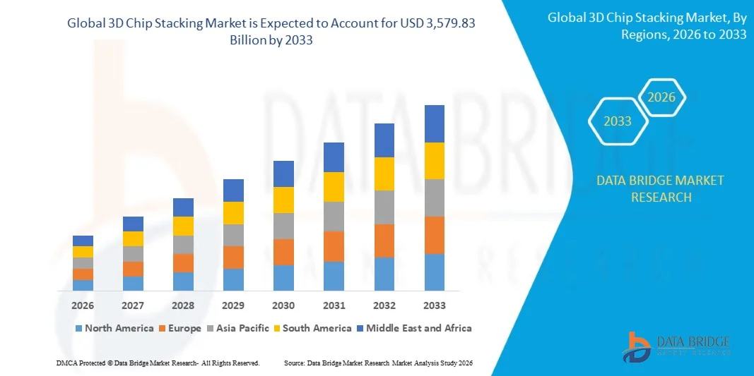
- As per Data Bridge Market Research analysis, the 3D chip stacking market was valued at USD 805.30 billion in 2025 and is projected to reach USD 3,579.83 billion by 2033, growing at a CAGR of 20.50% from 2026 to 2033.
- The market is experiencing rapid growth driven by surging demand for high-bandwidth memory in AI accelerator and data center processors, increasing adoption of advanced packaging as a substitute for continued transistor-level scaling, and growing integration of hybrid bonding technology enabling finer interconnect pitches and higher stacking density.
- The growing computational demands of generative AI training and inference workloads, combined with the slowing pace of traditional Moore's Law transistor scaling, is compelling semiconductor companies to pursue vertical die stacking as a primary pathway to increase compute density, reduce interconnect latency, and improve power efficiency. Rising adoption of high-bandwidth memory stacks paired with advanced logic dies is reshaping the architecture of next-generation AI and high-performance computing processors.
- Increasing collaboration between foundries, memory manufacturers, and outsourced semiconductor assembly and test providers is accelerating the commercialization of hybrid bonding and fine-pitch through-silicon via technologies, enabling higher-density, lower-latency chip stacks across logic, memory, and heterogeneous integration applications.
- Growing investment in chiplet-based design architectures is further reinforcing demand for 3D stacking technologies, as semiconductor companies increasingly combine specialized dies manufactured on different process nodes into a single vertically integrated package to optimize cost, performance, and time-to-market.
Market Size & Forecast
- Global Market Value (2025): USD 805.30 Billion
- Expected Market Value (2033): USD 3,579.83 Billion
- Forecast CAGR (2026–2033): 20.50%
- Leading Region in 2025: Asia-Pacific
- Fastest Growing Region: North America
What are the Major Takeaways of the 3D Chip Stacking Market?
- Asia-Pacific dominated the global 3D chip stacking market with the largest revenue share of 52.37% in 2025, supported by concentrated semiconductor foundry and advanced packaging capacity across Taiwan, South Korea, and China.
- North America is expected to be the fastest-growing region at a CAGR of 22.8% from 2026 to 2033, fueled by expanding domestic advanced packaging investment under national semiconductor initiatives and rising AI chip design activity among U.S.-based technology companies.
- The through-silicon via (TSV) technology segment led the market with a 44.62% share in 2025, driven by its established role as the foundational interconnect technology for high-bandwidth memory and logic-on-logic stacking applications.
- The hybrid bonding technology segment is the fastest-growing technology category, projected to register a CAGR of 25.4%, reflecting rising adoption of copper-to-copper direct bonding for ultra-fine-pitch, high-density chip stacking in AI accelerators.
- The memory (HBM/3D NAND) component type segment dominated the component category with a 48.93% revenue share in 2025, led by surging demand for high-bandwidth memory stacks paired with AI and high-performance computing processors.
- The AI & machine learning accelerators application segment accounted for 34.76% of the market share in 2025, preferred for its reliance on vertically stacked memory-logic architectures to meet extreme bandwidth and power-efficiency requirements.
- The die-to-wafer stacking approach is the fastest-growing stacking category, with a CAGR of 23.6%, driven by its balance of throughput and yield advantages for high-volume advanced packaging production.
Report Scope and 3D Chip Stacking Market Segmentation
|
Attributes |
3D Chip Stacking Key Market Insights |
|
Segments Covered |
|
|
Countries Covered |
North America
Europe
Asia-Pacific
Middle East and Africa
South America
|
|
Key Market Players |
|
|
Market Opportunities |
|
|
Value Added Data Infosets |
In addition to the insights on market scenarios such as market value, growth rate, segmentation, geographical coverage, and major players, the market reports curated by the Data Bridge Market Research also include in-depth expert analysis, geographically represented company-wise production and capacity, network layouts of distributors and partners, detailed and updated price trend analysis and deficit analysis of supply chain and demand. |
What is the Key Trend in the 3D Chip Stacking Market?
- Semiconductor manufacturers and foundries are increasingly adopting hybrid bonding technology to achieve sub-10-micron interconnect pitches, enabling significantly higher stacking density than conventional micro-bump approaches.
- For instance, in April 2025, TSMC expanded its System-on-Integrated-Chips advanced packaging capacity in Taiwan to support growing customer demand for hybrid-bonded logic and high-bandwidth memory stacking used in AI accelerator products.
- Rising adoption of high-bandwidth memory stacks incorporating eight and twelve-layer configurations is enabling memory manufacturers to deliver higher capacity and bandwidth within the same package footprint for AI training workloads.
- Foundries and outsourced semiconductor assembly and test providers are increasingly collaborating with memory manufacturers to co-develop integrated logic-memory stacking platforms optimized for next-generation AI processor architectures.
- For instance, in January 2025, SK hynix and a leading AI chip designer expanded their collaboration on next-generation high-bandwidth memory stacking, targeting improved bandwidth-per-watt performance for large-scale AI training clusters.
- As semiconductor companies continue to prioritize compute density, power efficiency, and interconnect bandwidth, the adoption of advanced 3D chip stacking technologies is expected to accelerate, reinforcing their role as a foundational technology for next-generation AI, high-performance computing, and data center processors.
What are the Key Drivers of the 3D Chip Stacking Market?
- The surging computational demands of generative AI training and inference workloads have significantly increased demand for high-bandwidth memory and logic stacking technologies capable of delivering extreme data throughput within constrained power envelopes.
- For instance, in March 2025, Samsung Electronics expanded its advanced packaging production capacity in South Korea to meet rising demand from AI chip customers requiring high-bandwidth memory and logic-stacking solutions.
- Semiconductor companies are increasingly incorporating 3D chip stacking into product roadmaps to overcome the diminishing returns of traditional transistor-level scaling, using vertical integration to improve performance without relying solely on smaller process nodes.
- For instance, in October 2024, Applied Materials announced an investment in additional hybrid bonding equipment manufacturing capacity to support rising orders from foundry and memory customers expanding advanced packaging production lines.
- With the semiconductor industry increasingly relying on advanced packaging to sustain performance scaling as transistor-level improvements slow, 3D chip stacking will remain indispensable across AI accelerators, high-performance computing processors, and next-generation memory products.
- For instance, in June 2024, Intel expanded its Foveros 3D packaging technology roadmap to support additional customer designs requiring vertically stacked logic and memory integration for client and data center processors.
Which Factors are Challenging the Growth of the 3D Chip Stacking Market?
- 3D chip stacking processes require significant capital investment in specialized bonding, thinning, and through-silicon via equipment, along with complex thermal management engineering to address heat dissipation challenges in densely stacked die configurations.
- These high capital costs and thermal-management complexity limit adoption among smaller semiconductor companies and constrain the entry of new players into advanced packaging manufacturing.
- For instance, in September 2024, SUSS MicroTec highlighted the increasing importance of hybrid bonding for advanced 3D stacking and HBM applications, while noting the growing equipment requirements associated with wafer thinning and hybrid-bonding processes.
- The high capital investment and yield-optimization complexity associated with advanced 3D chip stacking continue to restrict adoption, particularly among smaller semiconductor companies and emerging foundries. This cost and technical-complexity barrier slows market penetration beyond leading-edge processor and memory applications, limiting the widespread deployment of 3D stacking technologies despite growing performance demand.
How is the 3D Chip Stacking Market Segmented?
The 3D chip stacking market is segmented on the basis of technology, stacking approach, component type, application, end-use industry, layer count, substrate material, wafer size, interconnect pitch and packaging architecture.
- By Technology
On the basis of technology, the global 3D chip stacking market is segmented into through-silicon via (TSV), hybrid bonding, micro-bump/flip-chip stacking, wire bonding-based stacking, and monolithic 3D integration. The through-silicon via (TSV) segment dominated the market with a 44.62% share in 2025, owing to its established role as the foundational interconnect technology for high-bandwidth memory and logic-on-logic stacking applications. These interconnects deliver proven, high-density vertical electrical connections, making them the preferred choice for current-generation memory and logic stacking production.
The hybrid bonding segment is projected to register the fastest growth at a CAGR of 25.4% from 2026 to 2033, driven by rising adoption of copper-to-copper direct bonding for ultra-fine-pitch, high-density chip stacking in AI accelerators. Advances in wafer-surface preparation and bonding-alignment precision, combined with growing adoption among leading foundries, are accelerating segment expansion.
- By Stacking Approach
On the basis of stacking approach, the global 3D chip stacking market is segmented into wafer-to-wafer, die-to-wafer, and die-to-die. The wafer-to-wafer segment led the market with a 39.85% share in 2025, supported by its high-throughput production characteristics for homogeneous die stacking applications such as image sensors and memory.
The die-to-wafer segment is expected to experience the fastest growth at a CAGR of 23.6% from 2026 to 2033, driven by increasing demand for its balance of throughput and yield advantages, which allows known-good-die selection prior to stacking in high-value logic and memory applications.
- By Component Type
On the basis of component type, the global 3D chip stacking market is segmented into memory (HBM/3D NAND), logic ICs, image sensors, MEMS & sensors, and RF components. The memory (HBM/3D NAND) segment dominated the market with a share of 48.93% in 2025 due to its widespread adoption in high-bandwidth memory stacks paired with AI and high-performance computing processors, increasing demand for higher memory capacity within constrained package footprints, and growing integration with advanced logic dies. Additionally, rising focus on memory bandwidth and power efficiency further supports the strong adoption of stacked memory components.
The logic ICs segment is anticipated to witness the fastest CAGR of 22.9% from 2026 to 2033, driven by the increasing adoption of vertically stacked logic dies to overcome the diminishing performance gains of traditional transistor scaling. Manufacturers are adopting advanced packaging platforms to conduct cost-effective, scalable, and repeatable logic-die integration. Additionally, the integration of stacked logic with high-bandwidth memory is enhancing the performance and efficiency of next-generation AI processors, further driving segment growth.
- By Application
On the basis of application, the global 3D chip stacking market is segmented into high-performance computing, AI & machine learning accelerators, memory devices, mobile & consumer electronics, automotive electronics, and data center & networking. The AI & machine learning accelerators segment dominated the market with a share of 34.76% in 2025 due to its critical role in enabling extreme bandwidth and power-efficiency requirements for large-scale AI training and inference workloads. The widespread adoption of stacked high-bandwidth memory paired with advanced logic dies across AI accelerator platforms is driving strong demand for this application category.
The data center & networking segment is expected to witness the fastest CAGR of 23.1% from 2026 to 2033, driven by the rising need for higher-bandwidth, lower-latency interconnects within data center processors and networking silicon supporting growing cloud infrastructure demand. Manufacturers are increasingly integrating 3D stacked components into networking and server-processor designs. Additionally, the growing emphasis on data center energy efficiency is further accelerating adoption of this application category.
- By End-Use Industry
On the basis of end-use industry, the global 3D chip stacking market is segmented into consumer electronics, IT & telecommunications, automotive, healthcare, aerospace & defense, and industrial. The IT & telecommunications segment dominated the market with a share of 41.28% in 2025 due to its critical role in supporting cloud computing, data center, and AI infrastructure buildout requiring high-performance stacked semiconductor components. High adoption is driven by the increasing need for high-bandwidth, energy-efficient processors, integration with hyperscale data center architectures, and enhanced compute density. Additionally, growing investment by cloud service providers and semiconductor companies to improve AI infrastructure performance is reinforcing the leading position of this segment in the market.
The automotive segment is expected to witness the fastest CAGR of 23.8% from 2026 to 2033. This growth is driven by increasing adoption of advanced driver-assistance systems, autonomous driving platforms, and in-vehicle AI processing requiring compact, high-performance stacked semiconductor solutions. Growing integration of 3D stacked sensor and processing components in next-generation vehicle electronics is further accelerating market expansion in this segment.
- By Layer Count
On the basis of layer count, the global 3D chip stacking market is segmented into 2-4 layers, 5-8 layers, and 9+ layers. The 5-8 layers segment dominated the market with a share of 43.67% in 2025 due to its critical role in balancing memory capacity, thermal management, and manufacturing yield for current-generation high-bandwidth memory products. The widespread adoption of eight-layer high-bandwidth memory stacks across AI accelerator platforms is driving strong demand for this layer-count category.
The 9+ layers segment is expected to witness the fastest CAGR of 25.9% from 2026 to 2033, driven by the rising need for higher-capacity memory stacks capable of supporting increasingly data-intensive AI training workloads. Manufacturers are increasingly developing twelve-layer and higher-count stacking processes to push memory capacity and bandwidth further. Additionally, the growing emphasis on AI model size scaling is further accelerating adoption of this layer-count category.
- By Substrate Material
On the basis of substrate material, the global 3D chip stacking market is segmented into silicon, glass interposer, organic substrate, and others. The silicon segment dominated the market with a share of 56.84% in 2025 due to its widespread adoption as the established interposer and substrate material for high-density interconnect routing in advanced packaging applications. High adoption is supported by foundries and outsourced assembly providers that rely on proven silicon-interposer processes to ensure consistency, electrical performance, and measurable yield outcomes. Additionally, increasing integration with established silicon fabrication infrastructure enhances manufacturing scalability and reinforces the dominance of the silicon substrate segment.
The glass interposer segment is expected to witness the fastest CAGR of 24.7% from 2026 to 2033. This growth is primarily driven by the increasing demand for larger-format, lower-cost interposers with improved electrical and thermal properties compared to silicon for next-generation large-die AI accelerator packages. By offering superior dimensional stability and reduced signal loss at scale, this substrate material enhances package performance, cost efficiency, and manufacturing flexibility, making glass interposers highly attractive for large-format advanced packaging applications.
- By Wafer Size
On the basis of wafer size, the global 3D chip stacking market is segmented into 200 mm, 300 mm, and 450 mm. The 300 mm segment dominated the market with a share of 78.42% in 2025 due to its widespread adoption as the industry-standard wafer size across leading-edge semiconductor fabrication and advanced packaging facilities. Additionally, established equipment ecosystems, process standardization, and extensive fab-infrastructure compatibility are facilitating continued adoption of 300 mm wafer processing among semiconductor manufacturers, while strong supply-chain support networks are improving accessibility, reliability, and trust, further reinforcing this segment's leading market position.
The 200 mm segment is expected to witness the fastest CAGR of 12.6% from 2026 to 2033, driven by the increasing demand for legacy-node advanced packaging capacity supporting MEMS, RF, and specialty sensor stacking applications that do not require leading-edge process nodes. Manufacturers are leveraging existing 200 mm fab infrastructure to enhance cost efficiency, enable rapid capacity expansion, and support diverse specialty semiconductor packaging demand, thereby accelerating adoption across MEMS and sensor-focused advanced packaging applications.
- By Interconnect Pitch
On the basis of interconnect pitch, the global 3D chip stacking market is segmented into fine-pitch (<10 μm), standard pitch (10-40 μm), and coarse pitch (>40 μm). The standard pitch segment dominated the market with a share of 47.53% in 2025 due to its widespread use across current-generation high-bandwidth memory and logic stacking applications balancing interconnect density with manufacturing yield and cost. Additionally, established process maturity and broad equipment-supplier support are facilitating continued adoption of standard-pitch interconnects across mainstream advanced packaging production.
The fine-pitch segment is expected to witness the fastest CAGR of 26.3% from 2026 to 2033, driven by the increasing demand for higher interconnect density enabled by hybrid bonding technology in next-generation AI accelerator and high-bandwidth memory products. Manufacturers are leveraging advanced wafer-bonding and alignment technologies to enhance interconnect density, enable higher bandwidth per unit area, and support increasingly compact, high-performance chip stacks.
- By Packaging Architecture
On the basis of packaging architecture, the global 3D chip stacking market is segmented into 2.5D packaging and true 3D packaging. The 2.5D packaging segment dominated the market with a share of 61.72% in 2025 due to its critical role in providing a proven, high-yield packaging pathway that combines high-bandwidth memory and logic dies on a shared interposer without the full complexity of true vertical die-to-die stacking. Additionally, established process maturity across foundries and OSAT providers is facilitating continued adoption of 2.5D packaging across current-generation AI accelerator and high-performance computing products.
The true 3D packaging segment is expected to witness the fastest CAGR of 24.9% from 2026 to 2033, driven by the increasing demand for maximum interconnect density and minimum interconnect distance achievable only through direct vertical die-to-die or die-to-wafer stacking. Developers and foundries are leveraging hybrid bonding and advanced thermal-management techniques to enhance stacking density, enable higher performance per unit volume, and support next-generation AI and high-performance computing architectures, thereby accelerating adoption across leading-edge semiconductor applications.
Which Region Holds the Largest Share of the 3D Chip Stacking Market?
- Asia-Pacific dominated the 3D chip stacking market and accounted for the largest revenue share of 52.37% in 2025, supported by concentrated semiconductor foundry and advanced packaging capacity, strong presence of leading-edge chip manufacturers, and cost-competitive production capabilities across Taiwan, South Korea, and China.
- The region also benefits from extensive semiconductor fabrication and advanced packaging infrastructure, high adoption of hybrid bonding and TSV technologies, and growing use of 3D chip stacking across AI accelerator and high-bandwidth memory production applications. Increasing focus on export-oriented semiconductor manufacturing and rising domestic AI chip demand continues to strengthen Asia-Pacific's leadership position in the global market.
China 3D Chip Stacking Market Insight
The China 3D chip stacking market is expanding steadily, supported by growing domestic semiconductor manufacturing investment, rising demand for AI and data center processors, and increasing investment in domestic advanced packaging equipment development under national semiconductor self-reliance initiatives. Manufacturers are increasingly developing domestic TSV and advanced packaging capabilities for memory and logic stacking applications. Continuous expansion of domestic fabrication infrastructure and rising government support for advanced packaging equipment localization are further driving market growth in China.
Japan 3D Chip Stacking Market Insight
The Japan 3D chip stacking market is witnessing consistent growth due to rising investments in advanced semiconductor packaging technologies, precision manufacturing innovation, and strong domestic focus on materials and equipment supply for the global advanced packaging supply chain. Semiconductor equipment manufacturers, materials suppliers, and research institutes are increasingly developing high-precision bonding and wafer-thinning technologies supporting 3D chip stacking production. Moreover, increasing integration with global foundry and OSAT supply chains and the country's focus on manufacturing excellence are further contributing to market growth.
Europe 3D Chip Stacking Market Insight
Europe’s 3D chip stacking market is expanding rapidly, driven by AI, high-performance computing, automotive electronics, and advanced semiconductor packaging. Hybrid bonding, chiplets, and heterogeneous integration are key technologies enabling higher bandwidth, better energy efficiency, and compact designs. Europe benefits from strong semiconductor R&D, equipment expertise, and initiatives such as the EU Chips Act. Germany, France, Belgium, and the Netherlands are emerging as important hubs. Despite competition from Asia, increasing investment in advanced packaging creates significant opportunities through 2031 for equipment, materials, testing, and integration providers.
Germany 3D Chip Stacking Market Insight
The Germany 3D chip stacking market is expanding steadily due to the country's strong semiconductor equipment manufacturing base, growing automotive and industrial electronics demand, and increasing adoption of advanced packaging technologies among European chip manufacturers. Equipment manufacturers, semiconductor companies, and research institutes are increasingly collaborating on next-generation bonding and interconnect technologies. Continuous advancements in wafer-processing equipment, process automation, and quality-certification frameworks are further driving market growth in Germany.
France 3D Chip Stacking Market Insight
France is an emerging European hub for 3D chip stacking, supported by strong semiconductor R&D, advanced packaging expertise, and government-backed investment. Growth is driven by AI, high-performance computing, automotive electronics, and chiplet-based architectures. Research institutions and semiconductor companies are advancing hybrid bonding, wafer-level packaging, and heterogeneous integration technologies. France’s participation in the EU Chips Act strengthens its strategic position and supports domestic semiconductor capabilities. Key opportunities include advanced packaging equipment, materials, testing, thermal management, and chiplet integration.
Which are the Top Companies in 3D Chip Stacking Market?
The 3D chip stacking industry is primarily led by well-established companies, including:
- Taiwan Semiconductor Manufacturing Company Limited (Taiwan)
- Samsung Electronics Co., Ltd. (South Korea)
- Intel Corporation (U.S.)
- SK hynix Inc. (South Korea)
- Micron Technology, Inc. (U.S.)
- ASE Technology Holding Co., Ltd. (Taiwan)
- Amkor Technology, Inc. (U.S.)
- JCET Group Co., Ltd. (China)
- Applied Materials, Inc. (U.S.)
- Lam Research Corporation (U.S.)
- KLA Corporation (U.S.)
- Tokyo Electron Limited (Japan)
- BE Semiconductor Industries N.V. (Besi) (Netherlands)
- EV Group (EVG) (Austria)
- SUSS MicroTec SE (Germany)
- Onto Innovation Inc. (U.S.)
- GlobalFoundries Inc. (U.S.)
- United Microelectronics Corporation (Taiwan)
- Powertech Technology Inc. (Taiwan)
- DISCO Corporation (Japan)
- Advantest Corporation (Japan)
- Shinko Electric Industries Co., Ltd. (Japan)
- Ibiden Co., Ltd. (Japan)
- Kulicke & Soffa Industries, Inc. (Singapore)
- FormFactor, Inc. (U.S.)
- Brewer Science, Inc. (U.S.)
- Adeia Inc. (U.S.)
What are Latest Developments in 3D Chip Stacking Market?
- In September 2025, TSMC expanded its CoWoS and System-on-Integrated-Chips advanced packaging capacity in Taiwan to meet surging demand from AI accelerator customers requiring high-bandwidth memory and logic-stacking solutions.
- In February 2025, Samsung Electronics expanded its hybrid bonding production capacity in South Korea to support growing demand for next-generation high-bandwidth memory stacking from AI chip customers.
- In November 2025, Intel introduced an upgraded Foveros Direct hybrid bonding packaging platform incorporating finer interconnect pitches, improving stacking density and power efficiency for next-generation client and data center processors. This development strengthens Intel's position in the advanced packaging market by offering customers an alternative to conventional micro-bump stacking approaches.
- In October 2024, EV Group expanded its hybrid bonding equipment manufacturing capacity in Europe to include additional wafer-alignment and bonding system product lines, improving supply continuity for foundry and memory customers.
- In June 2023, Amkor Technology partnered with a leading AI chip designer to co-develop advanced 2.5D packaging solutions combining high-bandwidth memory and logic dies, combining its advanced packaging expertise with the partner's chip design requirements to support next-generation AI accelerator production.
- In March 2023, DISCO Corporation received manufacturing certification for an expanded wafer-thinning and dicing equipment production line dedicated to advanced packaging applications, enabling the company to serve growing demand from foundries and OSAT providers requiring ultra-thin die processing for high-layer-count stacking.
- Interactive Data Analysis Dashboard
- Company Analysis Dashboard for high growth potential opportunities
- Research Analyst Access for customization & queries
- Competitor Analysis with Interactive dashboard
- Latest News, Updates & Trend analysis
- Harness the Power of Benchmark Analysis for Comprehensive Competitor Tracking
Global 3d Chip Stacking Market, Supply Chain Analysis and Ecosystem Framework
To support market growth and help clients navigate the impact of geopolitical shifts, DBMR has integrated in-depth supply chain analysis into its Global 3d Chip Stacking Market research reports. This addition empowers clients to respond effectively to global changes affecting their industries. The supply chain analysis section includes detailed insights such as Global 3d Chip Stacking Market consumption and production by country, price trend analysis, the impact of tariffs and geopolitical developments, and import and export trends by country and HSN code. It also highlights major suppliers with data on production capacity and company profiles, as well as key importers and exporters. In addition to research, DBMR offers specialized supply chain consulting services backed by over a decade of experience, providing solutions like supplier discovery, supplier risk assessment, price trend analysis, impact evaluation of inflation and trade route changes, and comprehensive market trend analysis.
Data collection and base year analysis are done using data collection modules with large sample sizes. The stage includes obtaining market information or related data through various sources and strategies. It includes examining and planning all the data acquired from the past in advance. It likewise envelops the examination of information inconsistencies seen across different information sources. The market data is analysed and estimated using market statistical and coherent models. Also, market share analysis and key trend analysis are the major success factors in the market report. To know more, please request an analyst call or drop down your inquiry.
The key research methodology used by DBMR research team is data triangulation which involves data mining, analysis of the impact of data variables on the market and primary (industry expert) validation. Data models include Vendor Positioning Grid, Market Time Line Analysis, Market Overview and Guide, Company Positioning Grid, Patent Analysis, Pricing Analysis, Company Market Share Analysis, Standards of Measurement, Global versus Regional and Vendor Share Analysis. To know more about the research methodology, drop in an inquiry to speak to our industry experts.
Data Bridge Market Research is a leader in advanced formative research. We take pride in servicing our existing and new customers with data and analysis that match and suits their goal. The report can be customized to include price trend analysis of target brands understanding the market for additional countries (ask for the list of countries), clinical trial results data, literature review, refurbished market and product base analysis. Market analysis of target competitors can be analyzed from technology-based analysis to market portfolio strategies. We can add as many competitors that you require data about in the format and data style you are looking for. Our team of analysts can also provide you data in crude raw excel files pivot tables (Fact book) or can assist you in creating presentations from the data sets available in the report.