

What is the 3D Through-Silicon Via (TSV) Devices Market Size and Growth Rate?
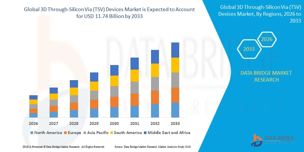
- As per Data Bridge Market Research analysis, the 3D through-silicon via (TSV) devices market was valued at USD 7.48 billion in 2025 and is projected to reach USD 11.74 billion by 2033, growing at a CAGR of 5.80% from 2026 to 2033.
- The market is experiencing consistent growth driven by rising demand for high-performance semiconductor devices, rapid advancements in 3D integrated circuit and advanced packaging technologies, and expanding applications across high-bandwidth memory, consumer electronics, artificial intelligence, and high-performance computing.
- The increasing adoption of AI and data-intensive computing, combined with growing demand for higher bandwidth, lower power consumption, and compact semiconductor architectures, is compelling semiconductor manufacturers to adopt advanced TSV technologies. 3D-stacked memory, heterogeneous integration, and wafer-level packaging are increasingly being used to improve device performance, connectivity, and integration density across emerging semiconductor applications.
Market Size & Forecast
- Global Market Value (2025): USD 7.48 Billion
- Expected Market Value (2033): USD 11.74 Billion
- Forecast CAGR (2026–2033): 5.80%
- Leading Region in 2025: North America
- Fastest Growing Region: Asia Pacific
What are the Major Takeaways of the 3D Through-Silicon Via (TSV) Devices Market?
- North America dominated the 3D through-silicon via (TSV) devices market with the largest revenue share of 34.40% in 2025, supported by strong investments in advanced semiconductor packaging, AI infrastructure, high-performance computing, and domestic semiconductor manufacturing capacity.
- Asia-Pacific is expected to be the fastest-growing region at a CAGR of 8.56% from 2026 to 2033, fueled by expanding semiconductor manufacturing capacity, rising HBM production, advanced packaging investments, and growing demand across China, South Korea, Japan, Taiwan, and India.
- The memory segment led the market with a 45.92% share in 2025, driven by the extensive use of TSV technology in high-bandwidth memory, stacked DRAM, and vertically integrated memory architectures
- MEMS and sensors are the fastest-growing product type, projected to register a CAGR of 8.57%, reflecting the surge in adoption of compact and highly integrated sensing components
- The via-middle TSV segment dominated the technology category with a 54.15% revenue share in 2025, led by its maturity in DRAM and CMOS image sensor applications.
- 3D IC packaging accounted for 65% of the market share in 2025, preferred by growing adoption of vertically integrated semiconductor architectures.
- The 2.5D packaging segment is the fastest-growing packaging type category, with a CAGR of 14%, driven by increasing adoption of chiplet-based architectures and advanced interposer technologies.
Report Scope and 3D Through-Silicon Via (TSV) Devices Market Segmentation
|
Attributes |
3D Through-Silicon Via (TSV) Devices Key Market Insights |
|
Segments Covered |
|
|
Countries Covered |
North America
Europe
Asia-Pacific
Middle East and Africa
South America
|
|
Key Market Players |
|
|
Market Opportunities |
|
|
Value Added Data Infosets |
In addition to the insights on market scenarios such as market value, growth rate, segmentation, geographical coverage, and major players, the market reports curated by the Data Bridge Market Research also include in-depth expert analysis, geographically represented company-wise production and capacity, network layouts of distributors and partners, detailed and updated price trend analysis and deficit analysis of supply chain and demand. |
What is the Key Trend in the 3D Through-Silicon Via (TSV) Devices Market?
- Semiconductor manufacturers are increasingly adopting TSV-enabled 3D stacking to integrate multiple memory and logic dies within compact packages, improving bandwidth, reducing interconnect distances, and supporting demanding AI and high-performance computing workloads.
- For instance, in March 2025, SK hynix announced that it had shipped the world’s first 12-layer HBM4 samples to major customers, with the product delivering more than 2 TB/s of bandwidth and using vertically stacked memory architecture for AI applications
- The growing use of high-bandwidth memory in AI accelerators is increasing demand for TSV-based vertical interconnects that provide high data-transfer performance while maintaining compact package dimensions.
- Advanced semiconductor manufacturers are also combining TSV-based 3D stacking with chiplet architectures and heterogeneous integration to improve computing performance, energy efficiency, and system-level integration.
- For instance, in February 2024, Micron Technology announced volume production of its HBM3E solution, developed using advanced TSV technology, delivering more than 1.2 TB/s of memory bandwidth and targeting AI accelerators, supercomputers, and data centers.
- As AI computing, HBM, chiplets, and advanced packaging continue to expand, TSV-based 3D integration is expected to become increasingly important for achieving higher bandwidth, lower latency, improved energy efficiency, and greater semiconductor integration density.
What are the Key Drivers of the 3D Through-Silicon Via (TSV) Devices Market?
- The rapid expansion of artificial intelligence and high-performance computing has significantly increased demand for high-bandwidth memory and advanced semiconductor architectures capable of handling intensive data-processing workloads with greater speed and energy efficiency.
- For instance, in February 2024, Micron Technology began volume production of its HBM3E solution for AI applications, using advanced TSV technology and 2.5D/3D stacking; the 24GB product delivered more than 1.2 TB/s of memory bandwidth and was designed for NVIDIA H200 GPUs.
- Semiconductor manufacturers, foundries, and memory companies are integrating TSV technology into increasingly sophisticated packaging architectures to connect vertically stacked dies and improve system performance without relying solely on conventional planar scaling.
- For instance, in August 2024, SK hynix highlighted its decade-long investment in TSV and advanced packaging technologies for HBM, noting that TSV-based HBM connects multiple DRAM chips to support high-speed data processing for AI workloads.
- With AI infrastructure, data centers, advanced processors, and high-bandwidth memory continuing to expand, TSV technology will remain an important enabler of 3D semiconductor integration, supporting higher computing density, faster data movement, and increasingly complex heterogeneous chip architectures.
What Factors are Challenging the Growth of the 3D Through-Silicon Via (TSV) Devices Market?
- Advanced TSV manufacturing requires complex wafer processing, precision etching, via formation, copper filling, wafer thinning, bonding, and inspection processes, increasing production complexity and manufacturing costs compared with conventional semiconductor packaging.
- For instance, in November 2024, a study published in Materials Science in Semiconductor Processing identified thermal stress as a major reliability challenge for copper-filled TSVs, noting that differences in thermal expansion between TSV layers can cause copper extrusion, interface damage, and performance degradation in 3D ICs.
- These technical requirements can create challenges related to yield, thermal management, wafer warpage, alignment accuracy, and reliability, particularly as manufacturers increase the number of vertically stacked dies and reduce individual die thickness.
- For instance, in December 2024, a study published in Advanced Engineering Materials highlighted continuing challenges related to TSV fabrication, filling processes, reliability, integration, packaging, and cost, demonstrating the technical complexity involved in scaling TSV-based 3D semiconductor architectures.
- The increasing process complexity and stringent reliability requirements associated with TSV-based 3D integration continue to challenge manufacturers, potentially increasing development costs, reducing manufacturing yields, and slowing adoption where advanced packaging infrastructure is limited.
How is the 3D Through-Silicon Via (TSV) Devices Market Segmented?
The 3D through-silicon via (TSV) devices market is segmented on the basis of product type, technology, packaging type, and end user.
- By Product Type
On the basis of product type, the 3D through-silicon via (TSV) devices market is segmented into memory, imaging and opto-electronics, MEMS and sensors, LED, and other products. The memory segment dominated the market with a 45.92% share in 2025, owing to the extensive use of TSV technology in high-bandwidth memory, stacked DRAM, and vertically integrated memory architectures. TSVs enable direct vertical connections between memory dies, improving bandwidth and reducing interconnect distances. The rapid expansion of artificial intelligence and high-performance computing is increasing demand for HBM-based memory solutions. Data-center processors and AI accelerators increasingly depend on high-bandwidth memory to handle intensive data workloads. Major memory manufacturers are consequently increasing their focus on higher-density stacked memory architectures.
The MEMS and sensors segment is projected to register the fastest growth at a CAGR of 8.57% during forecast period, driven by increasing adoption of compact and highly integrated sensing components. TSV technology enables vertical electrical connections that help reduce the footprint of MEMS and sensor packages. Automotive applications such as radar, inertial measurement, and advanced sensing are creating additional demand for TSV-enabled architectures. Consumer electronics are also incorporating increasing numbers of miniature sensors into connected devices and wearables. TSV integration can improve electrical connectivity while supporting smaller and more efficient device designs. Growing demand for miniaturized sensing solutions is therefore expanding the addressable market for TSV technology. The increasing use of MEMS and sensors across automotive, industrial, healthcare, and consumer applications is expected to sustain strong segment growth.
- By Technology
On the basis of technology, the 3D through-silicon via (TSV) devices market is segmented into via-middle TSV, via-last TSV, and via-first TSV. The via-middle TSV segment dominated the market with a 54.15% share in 2025, supported by its maturity in DRAM and CMOS image sensor applications. Via-middle TSVs are formed after transistor fabrication and before completion of the back-end interconnect structure. This positioning enables manufacturers to incorporate vertical interconnections while maintaining compatibility with established semiconductor processes. The technology is particularly suitable for stacked memory architectures requiring dense vertical connections. Its established manufacturing ecosystem and proven application base support continued commercial adoption.
The via-first TSV segment is projected to register the fastest growth at a CAGR of 7.69% during forecast period, driven by increasing adoption of chiplet-based and heterogeneous integration architectures. Via-first structures are formed earlier in the semiconductor fabrication process, allowing vertical interconnections to be incorporated into the device architecture from an earlier manufacturing stage. This approach is gaining relevance as semiconductor manufacturers pursue increasingly dense 3D integration. Chiplet architectures require precise interconnections between multiple processing and memory components. Improvements in wafer processing and alignment technologies are supporting broader implementation of via-first approaches. The technology is also relevant to advanced applications requiring compact and high-density vertical interconnects. Increasing demand for next-generation 3D semiconductor architectures is expected to support its rapid expansion.
- By Packaging Type
On the basis of packaging type, the 3D through-silicon via (TSV) devices market is segmented into 3D IC packaging, 2.5D packaging, wafer-level packaging, and other packaging types. The 3D IC packaging segment dominated the market with an estimated 65% share in 2025, supported by growing adoption of vertically integrated semiconductor architectures. 3D IC packaging enables multiple dies to be stacked within a compact package while TSVs provide high-density vertical electrical connections. HBM, AI processors, and high-performance computing systems are important applications supporting demand for this packaging approach. The technology enables shorter interconnect paths and higher integration density compared with conventional packaging architectures. Increasing demand for improved bandwidth and energy efficiency is encouraging semiconductor manufacturers to adopt advanced 3D packaging.
The 2.5D packaging segment is projected to register the fastest growth at a CAGR of 14% during forecast period, driven by increasing adoption of chiplet-based architectures and advanced interposer technologies. 2.5D packaging enables multiple heterogeneous dies to be integrated within a single package while maintaining high-bandwidth communication between components. The approach is increasingly used for AI accelerators, GPUs, high-performance processors, and data-center applications. Silicon interposers provide dense connections between processors and memory components without requiring complete vertical stacking of every die. This provides manufacturers with greater flexibility when integrating components manufactured using different process technologies. Growing chiplet adoption is further increasing demand for advanced interposer-based packaging solutions. The combination of high bandwidth, heterogeneous integration, and design flexibility is expected to drive strong growth in 2.5D packaging.
- By End User
On the basis of end user, the 3D through-silicon via (TSV) devices market is segmented into consumer electronics, automotive, IT and telecommunications, healthcare, aerospace and defense, industrial, and others. The IT and telecommunications segment dominated the market with a 37.54% share in 2025, supported by increasing demand for high-performance computing, data-center processors, networking equipment, and high-bandwidth memory. TSV-enabled devices allow semiconductor manufacturers to increase integration density while improving data-transfer performance. The rapid expansion of AI workloads is generating significant demand for processors paired with HBM architectures. Cloud computing and hyperscale data centers are also increasing their reliance on high-performance semiconductor packages. Growing deployment of GPUs, AI accelerators, and advanced networking processors is strengthening TSV adoption within this end-user category.
The automotive segment is projected to register the fastest growth at a CAGR of 9.08% during forecast period, driven by increasing semiconductor content in electric, connected, and software-defined vehicles. Modern vehicles require increasingly powerful processors and sensors for ADAS, automated driving, infotainment, and vehicle connectivity. TSV technology supports compact, high-performance semiconductor integration for applications requiring rapid data processing. Increasing deployment of automotive radar, imaging sensors, and advanced computing platforms is expanding demand for advanced semiconductor packaging. Electric vehicles are also increasing electronic content and computational requirements across vehicle architectures. TSV-enabled devices can help address requirements for high bandwidth, compact dimensions, and improved integration. Rising adoption of advanced automotive electronics is therefore expected to make automotive the fastest-growing end-user segment.
Which Region Holds the Largest Share of the 3D Through-Silicon Via (TSV) Devices Market?
- North America dominated the 3D through-silicon via (TSV) devices market with the largest revenue share of 34.40% in 2025, supported by strong investments in advanced semiconductor packaging, AI infrastructure, high-performance computing, and domestic semiconductor manufacturing capacity.
- The region also benefits from substantial investments in domestic semiconductor production, advanced HBM manufacturing, and government-supported semiconductor initiatives, alongside the presence of major technology and semiconductor companies. Increasing demand for AI accelerators, data-center infrastructure, and advanced 3D packaging technologies continues to strengthen North America's position in the global market
U.S. 3D Through-Silicon Via (TSV) Devices Market Insight
The U.S. 3D through-silicon via (TSV) devices market is witnessing strong growth due to rising investments in advanced semiconductor manufacturing, high-performance computing, and next-generation packaging technologies. The country’s strong semiconductor ecosystem, along with increasing adoption of HBM, 3D ICs, and chiplet-based architectures, is driving demand across data centers, consumer electronics, automotive, and aerospace applications. In addition, growing government and industry investments in domestic semiconductor production and advanced packaging infrastructure are accelerating TSV adoption across leading technology and semiconductor companies.
Asia-Pacific 3D Through-Silicon Via (TSV) Devices Market Insight
The Asia-Pacific 3D through-silicon via (TSV) devices market is expected to witness rapid growth, driven by expanding semiconductor manufacturing capabilities, increasing investments in advanced packaging, and rising demand for high-bandwidth memory across countries such as China, Japan, South Korea, and Taiwan. Growing adoption of 3D ICs, HBM, chiplet architectures, and wafer-level integration is supporting regional market expansion. Additionally, the strong presence of foundries, memory manufacturers, OSAT providers, and semiconductor equipment companies is accelerating TSV adoption across AI, HPC, consumer electronics, and automotive applications.
Japan 3D Through-Silicon Via (TSV) Devices Market Insight
The Japan 3D through-silicon via (TSV) devices market is witnessing consistent growth due to rising investments in semiconductor technology, advanced packaging, and next-generation memory solutions. Semiconductor manufacturers, electronics companies, and research institutions are increasingly adopting TSV technologies for 3D integration, image sensors, memory devices, and high-performance applications. Moreover, increasing investments in domestic semiconductor manufacturing and advanced packaging infrastructure, along with growing demand for compact and energy-efficient electronic systems, are further contributing to market growth in Japan.
China 3D Through-Silicon Via (TSV) Devices Market Insight
The China 3D through-silicon via (TSV) devices market is growing rapidly, driven by expanding semiconductor manufacturing capacity, increasing investments in advanced packaging, and rising demand for high-performance memory and computing technologies. Growing adoption of TSV-based 3D integration across memory, consumer electronics, artificial intelligence, and data-center applications is significantly boosting market demand. In addition, increasing efforts to strengthen domestic semiconductor capabilities, rising investments in chip packaging technologies, and rapid development of advanced memory solutions are positioning China as an important growth market for TSV devices globally.
U.K. 3D Through-Silicon Via (TSV) Devices Market Insight
The U.K. 3D through-silicon via (TSV) devices market is experiencing steady growth, supported by rising adoption of advanced semiconductor packaging, chiplet technologies, and high-performance computing solutions. Increasing investments in semiconductor research, photonics, artificial intelligence, and advanced electronic systems are contributing to market growth. Furthermore, integration of 3D stacking, heterogeneous integration, and advanced packaging technologies is improving device performance and energy efficiency, positioning the U.K. as an important research and innovation hub for next-generation semiconductor technologies.
Germany 3D Through-Silicon Via (TSV) Devices Market Insight
The Germany 3D through-silicon via (TSV) devices market is expanding steadily due to the country’s strong semiconductor ecosystem, advanced industrial capabilities, and increasing adoption of next-generation packaging technologies. Semiconductor companies, automotive manufacturers, research institutes, and electronics producers are increasingly utilizing advanced packaging and 3D integration for high-performance computing, automotive electronics, sensors, and industrial applications. Continuous advancements in heterogeneous integration, chiplet architectures, and high-density interconnect technologies, along with strong investment in semiconductor innovation, are further driving market growth in Germany.
Which are the Top Companies in 3D Through-Silicon Via (TSV) Devices Market?
The 3D through-silicon via (TSV) devices industry is primarily led by well-established companies, including:
- Taiwan Semiconductor Manufacturing Company Limited (Taiwan)
- Samsung Electronics Co., Ltd. (South Korea)
- Intel Corporation (U.S.)
- Micron Technology, Inc. (U.S.)
- SK hynix Inc. (South Korea)
- Toshiba Electronic Devices & Storage Corporation (Japan)
- ASE Technology Holding Co., Ltd. (Taiwan)
- Amkor Technology, Inc. (U.S.)
- United Microelectronics Corporation (Taiwan)
- STMicroelectronics N.V. (Switzerland)
- Broadcom Inc. (U.S.)
- Texas Instruments Incorporated (U.S.)
- GLOBALFOUNDRIES Inc. (U.S.)
- Advanced Micro Devices, Inc. (U.S.)
- Qualcomm Incorporated (U.S.)
- JCET Group Co., Ltd. (China)
- Powertech Technology Inc. (Taiwan)
- Nanya Technology Corporation (Taiwan)
- NEPES (South Korea)
- BE Semiconductor Industries N.V. (Netherlands)
What are Latest Developments in 3D Through-Silicon Via (TSV) Devices Market?
- In March 2025, SK hynix announced that it had shipped the world’s first 12-layer HBM4 samples to major customers, incorporating advanced packaging technologies for next-generation AI memory. The HBM4 product uses vertically stacked DRAM architecture and advanced MR-MUF technology, strengthening the role of TSV-based 3D integration in high-performance AI and data-center applications
- In September 2024, SK hynix announced the start of volume production of its 12-layer HBM3E, featuring 36GB capacity and vertically stacked DRAM chips enabled by TSV technology. The development involved making individual DRAM chips thinner while maintaining package height, demonstrating continued advances in TSV-based high-density 3D memory packaging for AI applications.
- In February 2024, Micron announced the start of volume production of its HBM3E solution, developed using advanced through-silicon via (TSV) technology and 2.5D/3D-stacking techniques. The HBM3E solution was designed for AI accelerators and data-center applications, with the 24GB product planned for integration into NVIDIA H200 Tensor Core GPUs, highlighting the growing adoption of TSV-based memory architectures.
- In April 2023, SK hynix announced the development of the industry’s first 12-layer HBM3 with 24GB capacity and provided samples to customers for performance evaluation. The product applied TSV technology to vertically connect the DRAM chips while reducing individual chip thickness, supporting higher-density memory packaging for rapidly expanding AI and high-performance computing applications.
- In June 2022, SK hynix announced the start of mass production of HBM3 DRAM and its supply for NVIDIA H100 Tensor Core GPUs. The HBM3 architecture vertically interconnected multiple DRAM chips using TSV technology to deliver higher bandwidth and density, marking an important commercial development for TSV-based 3D memory and advanced semiconductor packaging.
- Interactive Data Analysis Dashboard
- Company Analysis Dashboard for high growth potential opportunities
- Research Analyst Access for customization & queries
- Competitor Analysis with Interactive dashboard
- Latest News, Updates & Trend analysis
- Harness the Power of Benchmark Analysis for Comprehensive Competitor Tracking
Global 3d Through Silicon Via Tsv Devices Market, Supply Chain Analysis and Ecosystem Framework
To support market growth and help clients navigate the impact of geopolitical shifts, DBMR has integrated in-depth supply chain analysis into its Global 3d Through Silicon Via Tsv Devices Market research reports. This addition empowers clients to respond effectively to global changes affecting their industries. The supply chain analysis section includes detailed insights such as Global 3d Through Silicon Via Tsv Devices Market consumption and production by country, price trend analysis, the impact of tariffs and geopolitical developments, and import and export trends by country and HSN code. It also highlights major suppliers with data on production capacity and company profiles, as well as key importers and exporters. In addition to research, DBMR offers specialized supply chain consulting services backed by over a decade of experience, providing solutions like supplier discovery, supplier risk assessment, price trend analysis, impact evaluation of inflation and trade route changes, and comprehensive market trend analysis.
Data collection and base year analysis are done using data collection modules with large sample sizes. The stage includes obtaining market information or related data through various sources and strategies. It includes examining and planning all the data acquired from the past in advance. It likewise envelops the examination of information inconsistencies seen across different information sources. The market data is analysed and estimated using market statistical and coherent models. Also, market share analysis and key trend analysis are the major success factors in the market report. To know more, please request an analyst call or drop down your inquiry.
The key research methodology used by DBMR research team is data triangulation which involves data mining, analysis of the impact of data variables on the market and primary (industry expert) validation. Data models include Vendor Positioning Grid, Market Time Line Analysis, Market Overview and Guide, Company Positioning Grid, Patent Analysis, Pricing Analysis, Company Market Share Analysis, Standards of Measurement, Global versus Regional and Vendor Share Analysis. To know more about the research methodology, drop in an inquiry to speak to our industry experts.
Data Bridge Market Research is a leader in advanced formative research. We take pride in servicing our existing and new customers with data and analysis that match and suits their goal. The report can be customized to include price trend analysis of target brands understanding the market for additional countries (ask for the list of countries), clinical trial results data, literature review, refurbished market and product base analysis. Market analysis of target competitors can be analyzed from technology-based analysis to market portfolio strategies. We can add as many competitors that you require data about in the format and data style you are looking for. Our team of analysts can also provide you data in crude raw excel files pivot tables (Fact book) or can assist you in creating presentations from the data sets available in the report.