

What is the Direct Write Semiconductor Market Size and Growth Rate?
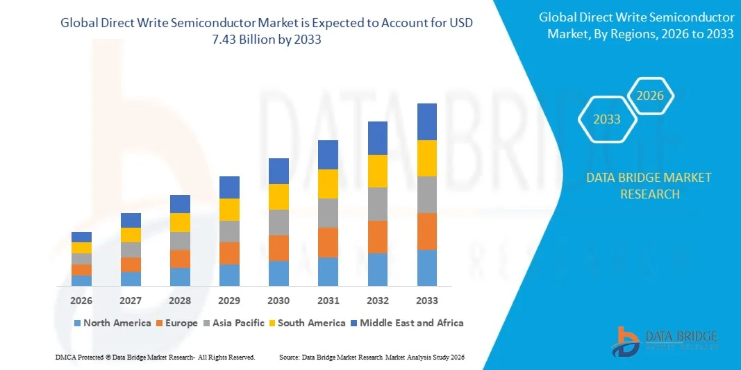
- As per market analysis, the global Direct Write Semiconductor Market was valued at approximately USD 5.62 billion in 2025 and is projected to reach USD 7.43 billion by 2033, growing at a CAGR of 7.60% from 2026 to 2033.
- The market is witnessing growth driven by increasing demand for advanced semiconductor manufacturing, rapid prototyping, customized electronic devices, miniaturized semiconductor components, and flexible fabrication processes. Direct write technologies enable localized and maskless patterning, supporting applications across semiconductor devices, microelectronics, sensors, MEMS, and advanced electronic components.
- Increasing adoption of AI-enabled electronics, Internet of Things (IoT) devices, advanced sensors, flexible electronics, and next-generation semiconductor architectures is creating further growth opportunities. Growing requirements for customized device structures, reduced fabrication cycles, rapid design iteration, and cost-efficient prototyping are supporting market development across semiconductor manufacturing, electronics, MEMS, sensors, and research applications.
Market Size & Forecast
- Market Value (2025): USD 5.62 billion
- Expected Market Value (2033): USD 7.43 Million
- Forecast CAGR (2026–2033): 7.60%
- Leading Region in 2025: North America
- Fastest Growing Region: Asia-Pacific
What are the Major Takeaways of the Direct Write Semiconductor Market?
- North America dominated the global Direct Write Semiconductor Market share of 44.12% in 2025, supported by its advanced semiconductor manufacturing ecosystem, strong R&D infrastructure, presence of leading technology and semiconductor equipment companies, and increasing investment in maskless lithography and advanced packaging technologies. The region's established semiconductor industry and government-backed initiatives supporting domestic chip manufacturing are further contributing to market development.
- Asia Pacific is expected to witness the fastest growth in the global Direct Write Semiconductor Market CAGR of 7.34%, driven by expanding semiconductor production capacity, increasing investments in China, Japan, South Korea, and Taiwan, rising demand for advanced electronics, and growing adoption of direct-write technologies for miniaturized and customized semiconductor components. Public market analysis projects Asia Pacific to register an 8.77% CAGR from 2026 to 2033.
- Electron Beam Direct Write represented the leading technology segment, accounting for a 48.11% revenue share in 2025, supported by its high precision, superior resolution, and suitability for integrated circuits, photonic devices, and advanced semiconductor patterning.
- IC Packaging represented the leading application segment, accounting for a 39.04% revenue share in 2025, supported by increasing demand for compact, high-performance semiconductor packages, advanced interconnects, and miniaturized electronic components.
- Metal Inks represented the leading material segment, accounting for a 45.17% revenue share in 2025, supported by their high electrical conductivity, printability, and suitability for producing fine conductive patterns in semiconductor and electronic applications.
Report Scope Direct Write Semiconductor Market Segmentation
|
Attributes |
Direct Write Semiconductor Market Key Market Insights |
|
Segments Covered |
|
|
Countries Covered |
North America
Europe
Asia-Pacific
Middle East and Africa
South America
|
|
Key Market Players |
|
|
Market Opportunities |
|
|
Value Added Data Infosets |
In addition to the insights on market scenarios such as market value, growth rate, segmentation, geographical coverage, and major players, the market reports curated by the Data Bridge Market Research also include in-depth expert analysis, geographically represented company-wise production and capacity, network layouts of distributors and partners, detailed and updated price trend analysis and deficit analysis of supply chain and demand. |
What is the Key Trend in the Direct Write Semiconductor Market?
- Increasing adoption of maskless direct-write technologies for rapid prototyping, customized semiconductor fabrication, and advanced packaging is emerging as a key trend in the market. Semiconductor manufacturers, research institutions, and fabless companies are increasingly adopting direct-write electron-beam and laser-based systems to reduce dependence on conventional photomasks, accelerate design iterations, and support low-volume or specialized semiconductor production. The technology is particularly relevant for advanced packaging, photonic devices, MEMS, sensors, compound semiconductors, and other applications requiring high patterning flexibility.
- For instance, in August 2025, Multibeam and SecureFoundry introduced maskless electron-beam lithography tools designed for direct wafer writing. The systems were developed to enable rapid and customized chip prototyping while reducing the dependence on expensive traditional masks. The development highlights the increasing use of direct-write technologies for faster design validation and specialized semiconductor fabrication.
- The trend is expected to remain important as semiconductor development increasingly requires faster prototyping, design flexibility, and cost-efficient patterning. Direct-write systems enable digital pattern modification without requiring a new physical photomask, making them suitable for low-volume production, research, and advanced device development. Demand is also being supported by the expansion of advanced packaging and heterogeneous integration, where finer patterns and flexible fabrication processes are increasingly required.
- The growing emphasis on advanced packaging and specialized semiconductor fabrication is further influencing direct-write technology development, with laser-based and electron-beam systems increasingly being applied to photonic devices, sensors, compound semiconductors, IC packaging, and heterogeneous integration.
What are the Key Drivers of the Direct Write Semiconductor Market?
- Increasing demand for faster, flexible, and cost-efficient semiconductor manufacturing is emerging as a key driver of the Global Direct Write Semiconductor Market. Direct write technologies enable digital patterns to be transferred directly onto substrates without requiring physical photomasks, supporting faster design modifications, reducing tooling requirements, and improving manufacturing flexibility. These capabilities are particularly relevant for semiconductor development, prototyping, pilot production, advanced packaging, MEMS, sensors, and other high-mix applications.
- For instance, in October 2024, Nikon introduced its DSP-100 digital lithography solution for advanced semiconductor packaging. The system uses a spatial light modulator to directly write patterns onto substrates without conventional physical photomasks. The development reflects the industry's increasing adoption of maskless patterning technologies to improve precision, design flexibility, and production efficiency in advanced semiconductor applications.
- The growing adoption of rapid prototyping and customized semiconductor development is further supporting market growth. Direct write technologies allow manufacturers and research organizations to modify digital layouts and produce new patterns without fabricating a new photomask for each design iteration. This reduces development cycles and supports low-volume, high-complexity, and customized semiconductor applications. Heidelberg Instruments highlights faster design iterations, shorter development cycles, and greater patterning flexibility as key benefits of maskless lithography.
- The expansion of advanced packaging, heterogeneous integration, photonics, MEMS, and flexible electronics is creating additional demand for direct write solutions. Increasing device miniaturization and the development of complex architectures require high-resolution patterning across different substrates and materials. Direct write systems provide the flexibility required for rapid experimentation and fabrication of intricate structures, supporting their use across emerging microelectronics and semiconductor applications.
- Increasing integration of automation, advanced process control, and high-resolution patterning technologies is expected to remain an important driver. Electron-beam and laser-based direct write systems are being developed with higher throughput, improved resolution, automation, and process monitoring capabilities. These developments are helping address productivity requirements while maintaining the precision required for semiconductor and nanofabrication applications.
Which Factors are Challenging the Growth of the Direct Write Semiconductor Market?
- High Initial Capital Expenditure and Equipment Costs are emerging as a key challenge in the Global Direct Write Semiconductor Market. Direct write technologies require specialized laser, electron beam, material deposition, alignment, and process-control systems, which involve significant upfront investment. The cost of advanced equipment can create barriers for small and medium-sized semiconductor manufacturers, research organizations, and facilities operating with limited capital budgets. Global Market Insights identifies high initial capital expenditure and equipment costs as a major challenge for the market.
- For instance, in June 2026, direct write systems must deliver high-resolution patterning, precise alignment, substrate handling, and reliable process control across different semiconductor applications. Heidelberg Instruments highlights that complex multilayer fabrication requires accurate registration, process optimization, and adaptation to challenging substrates such as warped wafers, thin foils, and surfaces with existing topography. These requirements increase system complexity and can raise equipment acquisition and integration costs.
- The challenge is further intensified by throughput and scalability requirements in semiconductor manufacturing. Conventional photolithography remains cost-effective for high-volume production because mask costs can be distributed across large production volumes, while direct write is particularly advantageous for research, prototyping, high-mix, and low-volume manufacturing. Therefore, direct write technology must continue improving writing speed, throughput, overlay accuracy, and automation to become more competitive across larger-scale semiconductor production environments.
- Limited standardization of direct write processes also remains a challenge as manufacturers use different technologies, materials, substrates, and process configurations. Variations in laser-based, electron-beam, and material-deposition approaches can require application-specific optimization and integration with existing semiconductor manufacturing workflows. This can increase qualification time, process-development requirements, and adoption complexity.
How is the Direct Write Semiconductor Market Segmented?
The market is segmented on the basis of technology, application, material, substrate, and process type.
- By Technology
On the basis of technology, the global Direct Write Semiconductor Market is segmented into Laser-Based Direct Write, Electron Beam Direct Write, and Chemical Direct Write. The Electron Beam Direct Write segment dominated the market with a 48.11% revenue share in 2025, supported by its high precision, resolution, and ability to produce intricate patterns for semiconductor devices, integrated circuits, and photonic applications. Electron beam technology is particularly suitable for applications requiring high-resolution patterning and precise feature definition.
The Laser-Based Direct Write segment is expected to witness the fastest growth during the forecast period, registering a CAGR of 8.37% from 2026 to 2033, supported by increasing adoption of fast, non-contact, maskless patterning technologies. The technology is gaining application across flexible electronics, microelectronics, automotive electronics, and other applications requiring rapid and precise patterning.
- By Application
On the basis of application, the global Direct Write Semiconductor Market is segmented into IC Packaging, Photonic Devices, Sensor Fabrication, and Display Fabrication. The IC Packaging segment dominated the market with a 39.04% revenue share in 2025, supported by increasing demand for compact, high-performance semiconductor components and advanced packaging technologies. Direct write processes enable maskless and precise patterning for complex interconnects and packaging structures, supporting the development of advanced semiconductor packages.
The Photonic Devices segment is expected to witness the fastest growth during the forecast period with a CAGR of 8.82% from 2026 to 2033, driven by increasing demand for high-speed optical communication, data transmission, photonic computing, and advanced optical components. The expansion of AI and data-center infrastructure is further supporting demand for photonic devices requiring highly precise fabrication processes.
- By Material
On the basis of material, the global Direct Write Semiconductor Market is segmented into Metal Inks, Ceramic Inks, and Polymer Inks. The Metal Inks segment dominated the market with a 45.17% revenue share in 2025, supported by their high electrical conductivity, printability, and suitability for producing fine conductive tracks and electronic structures. Metal-based materials are widely used in direct-write applications requiring efficient electrical connections and high-resolution conductive patterns.
The Ceramic Inks segment is expected to witness the fastest growth during the forecast period with a CAGR of 8.13% from 2026 to 2033, supported by increasing demand for high-resolution, durable, and thermally stable printed structures. Growing requirements for miniaturized semiconductor components and complex electronic designs are further supporting the adoption of ceramic-based materials in direct-write processes.
- By Substrate
On the basis of substrate, the global Direct Write Semiconductor Market is segmented into Silicon, Glass, Metal, and Composite Materials. The Silicon segment dominated the market with a 36.17% revenue share in 2025, supported by the extensive use of silicon in microelectronics and semiconductor manufacturing. High reliability, established manufacturing infrastructure, and compatibility with semiconductor fabrication processes continue to support the use of silicon substrates in direct-write applications.
The Glass segment is expected to witness the fastest growth during the forecast period with a CAGR of 9.12% from 2026 to 2033, driven by increasing adoption of glass substrates in flexible electronics, displays, photonic components, and lightweight electronic devices. The combination of mechanical strength, optical properties, and compatibility with advanced electronic structures is supporting greater application of glass substrates.
- By Process Type
On the basis of process type, the global Direct Write Semiconductor Market is segmented into Single-Step Direct Write and Multi-Step Direct Write. The Single-Step Direct Write segment dominated the market with a 67.91% revenue share in 2025, supported by simplified processing, shorter production times, and suitability for low-volume manufacturing and rapid prototyping. The approach provides manufacturers with greater flexibility for customized semiconductor structures while reducing the number of processing stages.
The Multi-Step Direct Write segment is expected to witness the fastest growth during the forecast period with a CAGR of 8.31% from 2026 to 2033, supported by its ability to enable complex, multilayer, and highly precise semiconductor structures. Increasing demand for advanced packaging, multi-material electronics, and complex device architectures is expected to support adoption of multi-step direct-write processes.
Which Region Holds the Largest Share of the Direct Write Semiconductor Market?
- North America dominated the global Direct Write Semiconductor Market, accounting for a 39.51% revenue share in 2025, supported by strong semiconductor research and development activities, advanced manufacturing infrastructure, government-backed semiconductor investments, and the presence of major technology and semiconductor companies. The region, particularly the U.S., has benefited from initiatives such as the CHIPS Act, which has supported domestic semiconductor manufacturing, advanced packaging, and next-generation fabrication technologies.
- Asia Pacific is expected to witness the fastest growth in the global Direct Write Semiconductor Market during the forecast period, at a CAGR of 8.77% from 2026 to 2033, driven by increasing semiconductor production in China, Japan, South Korea, and Taiwan. The region is benefiting from expanding semiconductor fabrication capacity, investments in advanced manufacturing technologies, growing demand for miniaturized electronic components, and increasing adoption of direct-write and maskless patterning technologies for advanced packaging, photonic devices, sensors, and other semiconductor applications.
U.S. Direct Write Semiconductor Market Insight
The U.S. Direct Write Semiconductor Market is expanding with increasing demand for rapid semiconductor prototyping, advanced packaging, maskless lithography, and low-volume customized chip development. The country is also benefiting from investments in advanced packaging, heterogeneous integration, and semiconductor fabrication infrastructure. In 2025, the U.S. Department of Commerce finalized USD 1.4 billion in NAPMP awards to strengthen domestic advanced packaging capabilities, supporting opportunities for direct-write technologies.
Europe Direct Write Semiconductor Market Insight
Europe is emerging as an important market for direct-write semiconductor technologies, supported by semiconductor R&D, advanced lithography capabilities, and policy initiatives aimed at strengthening regional chip manufacturing. The European Chips Act and related investments are supporting advanced fabrication, packaging, and next-generation patterning technologies. Demand is further supported by applications in photonics, sensors, advanced packaging, and specialized semiconductor prototyping.
U.K. Direct Write Semiconductor Market Insight
The U.K. Direct Write Semiconductor Market is supported by the country’s established semiconductor design, photonics, microelectronics, and advanced manufacturing ecosystem. Growing investments in semiconductor research, compound semiconductors, photonic devices, and heterogeneous integration are creating opportunities for direct-write technologies used in prototyping, sensor fabrication, IC packaging, and advanced electronic structures. Demand is further supported by the development of high-performance computing, communications, automotive electronics, and specialized semiconductor applications. Collaboration among universities, research institutions, technology companies, and semiconductor manufacturers is also supporting innovation and adoption of advanced direct-write fabrication techniques.
Germany Direct Write Semiconductor Market Insight
Germany’s Direct Write Semiconductor Market is supported by its strong semiconductor equipment ecosystem, advanced manufacturing capabilities, and established research infrastructure. The country benefits from the presence of specialized technology providers and research institutions involved in electron-beam lithography, laser-based patterning, microfabrication, and semiconductor process development. Growing demand for advanced packaging, photonic devices, sensors, and miniaturized electronic components is creating opportunities for direct-write technologies. Increasing investments in semiconductor manufacturing and next-generation microelectronics are further supporting market development, while Germany’s emphasis on precision engineering and high-value industrial applications strengthens adoption across advanced semiconductor fabrication and prototyping.
Asia-Pacific Direct Write Semiconductor Market Insight
The Asia-Pacific Direct Write Semiconductor Market is experiencing increasing adoption due to the region’s expanding semiconductor manufacturing ecosystem, advanced electronics production, and growing investments in next-generation fabrication technologies. Countries such as China, Japan, South Korea, and Taiwan are strengthening semiconductor capabilities through investments in advanced packaging, photonic devices, sensors, and miniaturized electronic components. Direct-write technologies are gaining traction because they enable maskless patterning, rapid prototyping, design flexibility, and precise fabrication. Rising demand for consumer electronics, automotive semiconductors, data-center infrastructure, and advanced semiconductor devices is expected to further support regional market growth.
Japan Direct Write Semiconductor Market Insight
Japan’s Direct Write Semiconductor Market is supported by the country’s strong semiconductor equipment ecosystem, advanced materials capabilities, precision manufacturing expertise, and growing investment in domestic semiconductor technologies. Demand is being supported by applications in semiconductor R&D, advanced packaging, photonic devices, MEMS, and sensor fabrication. Electron beam direct-write technology remains important for high-resolution prototyping, while laser-based digital lithography is gaining traction in advanced packaging.
China Direct Write Semiconductor Market Insight
China’s Direct Write Semiconductor Market is supported by expanding semiconductor manufacturing capacity, increasing investment in domestic semiconductor equipment, and the country’s focus on strengthening its self-sufficient chip supply chain. Growing investments in wafer fabrication, advanced packaging, MEMS, and display manufacturing are creating demand for direct-write lithography solutions. Domestic equipment development is also progressing, with Chinese companies expanding capabilities in direct-writing lithography for IC, packaging, MEMS, and related applications.
Which are the Top Companies in Direct Write Semiconductor Market?
The Direct Write Semiconductor Market industry is primarily led by well-established companies, including:
- Heidelberg Instruments Mikrotechnik GmbH (Germany)
- Raith GmbH (Germany)
- Vistec Electron Beam GmbH (Germany)
- JEOL Ltd. (Japan)
- Nanoscribe GmbH & Co. KG (Germany)
- Elionix Inc. (Japan)
- SÜSS MicroTec SE (Germany)
- Optomec Inc. (U.S.)
- Eulitha AG (Switzerland)
- Crestec Corporation (Japan)
- KLOE SAS (France)
- Holmarc Opto-Mechatronics Ltd. (India)
- Microlight3D SAS (France)
- NanoSystem Solutions, Inc. (Japan)
- SVG Optronics Co., Ltd. (China)
What are Latest Developments in Direct Write Semiconductor Market?
- In June 2026, Nikon announced the development of a new digital lithography system for advanced semiconductor packaging. The system is designed to provide 1.5 µm resolution and target throughput of 65 panels per hour or higher, compared with 50 panels per hour for its DSP-100. The system is scheduled for release in fiscal year 2027.
- In August 2025, U.S.-based Multibeam and SecureFoundry introduced maskless electron-beam lithography tools designed for direct wafer writing. The technology is intended to support rapid and customized chip prototyping while reducing dependence on conventional photomasks.
- In September 2025, MetaOptics deployed its Direct Laser Writer system at Pin-Jye Nano Technologies in Taoyuan, Taiwan. The deployment supports the commercialization of maskless direct laser writing for metalens manufacturing and advanced optical applications.
- In 2025, Heidelberg Instruments introduced a higher-speed MLA 300 model with 3 µm resolution, with initial systems shipped and installed. The company also indicated plans for a 1.5 µm-resolution system targeting 2027, reflecting increasing demand for direct-write solutions in advanced packaging and lower-volume production.
- In 2026, Multibeam announced a USD 140 million Letter of Intent with the U.S. Department of Commerce for a strategic initiative focused on fine-pitch process flows for next-generation heterogeneous chip integration. The initiative targets direct-write electron-beam lithography for advanced integration, photonics, quantum technologies, and other microelectronics applications.
- Interactive Data Analysis Dashboard
- Company Analysis Dashboard for high growth potential opportunities
- Research Analyst Access for customization & queries
- Competitor Analysis with Interactive dashboard
- Latest News, Updates & Trend analysis
- Harness the Power of Benchmark Analysis for Comprehensive Competitor Tracking
Global Direct Write Semiconductor Market, Supply Chain Analysis and Ecosystem Framework
To support market growth and help clients navigate the impact of geopolitical shifts, DBMR has integrated in-depth supply chain analysis into its Global Direct Write Semiconductor Market research reports. This addition empowers clients to respond effectively to global changes affecting their industries. The supply chain analysis section includes detailed insights such as Global Direct Write Semiconductor Market consumption and production by country, price trend analysis, the impact of tariffs and geopolitical developments, and import and export trends by country and HSN code. It also highlights major suppliers with data on production capacity and company profiles, as well as key importers and exporters. In addition to research, DBMR offers specialized supply chain consulting services backed by over a decade of experience, providing solutions like supplier discovery, supplier risk assessment, price trend analysis, impact evaluation of inflation and trade route changes, and comprehensive market trend analysis.
Data collection and base year analysis are done using data collection modules with large sample sizes. The stage includes obtaining market information or related data through various sources and strategies. It includes examining and planning all the data acquired from the past in advance. It likewise envelops the examination of information inconsistencies seen across different information sources. The market data is analysed and estimated using market statistical and coherent models. Also, market share analysis and key trend analysis are the major success factors in the market report. To know more, please request an analyst call or drop down your inquiry.
The key research methodology used by DBMR research team is data triangulation which involves data mining, analysis of the impact of data variables on the market and primary (industry expert) validation. Data models include Vendor Positioning Grid, Market Time Line Analysis, Market Overview and Guide, Company Positioning Grid, Patent Analysis, Pricing Analysis, Company Market Share Analysis, Standards of Measurement, Global versus Regional and Vendor Share Analysis. To know more about the research methodology, drop in an inquiry to speak to our industry experts.
Data Bridge Market Research is a leader in advanced formative research. We take pride in servicing our existing and new customers with data and analysis that match and suits their goal. The report can be customized to include price trend analysis of target brands understanding the market for additional countries (ask for the list of countries), clinical trial results data, literature review, refurbished market and product base analysis. Market analysis of target competitors can be analyzed from technology-based analysis to market portfolio strategies. We can add as many competitors that you require data about in the format and data style you are looking for. Our team of analysts can also provide you data in crude raw excel files pivot tables (Fact book) or can assist you in creating presentations from the data sets available in the report.