
Global E Beam Wafer Inspection System Market
Market Size in USD Billion
 USD
1.37 Billion
USD
5.23 Billion
2025
2033
USD
1.37 Billion
USD
5.23 Billion
2025
2033
| 2026 - 2033 | |
| USD 1.37 Billion | |
| USD 5.23 Billion | |
| % | |
|
E-Beam Wafer Inspection System Market Size
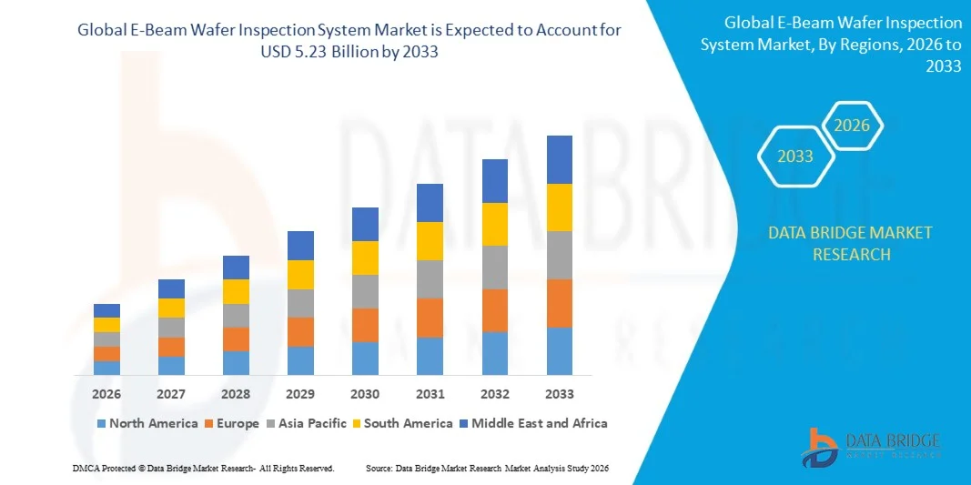
- The global e-beam wafer inspection system market size was valued at USD 1.37 billion in 2025 and is expected to reach USD 5.23 billion by 2033, at a CAGR of 18.25% during the forecast period
- The market growth is largely fueled by the increasing complexity of semiconductor devices and the transition toward advanced process nodes, which require highly precise defect detection capabilities to maintain yield and performance
- Furthermore, rising demand for high-performance chips across applications such as artificial intelligence, automotive electronics, and data centers is driving the need for advanced inspection systems. These converging factors are accelerating the adoption of e-beam wafer inspection technologies, thereby significantly boosting the market growth
E-Beam Wafer Inspection System Market Analysis
- E-beam wafer inspection systems utilize focused electron beams to scan semiconductor wafers for detecting nanoscale defects with extremely high resolution. These systems play a critical role in process control, yield enhancement, and quality assurance in advanced semiconductor manufacturing
- The escalating demand for these systems is primarily driven by shrinking node sizes, increasing adoption of EUV lithography, and the growing need for accurate detection of complex and buried defects that cannot be identified using traditional optical inspection methods
- Asia-Pacific dominated the e-beam wafer inspection system market with a share of 33.5% in 2025, due to the strong presence of semiconductor manufacturing hubs, increasing investments in advanced fabrication facilities, and rising demand for high-performance chips across consumer electronics and automotive sectors
- North America is expected to be the fastest growing region in the e-beam wafer inspection system market during the forecast period due to strong investments in semiconductor manufacturing, increasing demand for advanced chips, and government initiatives supporting domestic production
- 300-mm wafers segment dominated the market with a market share of 53.1% in 2025, due to its extensive adoption in advanced semiconductor manufacturing for high-volume production. Foundries and integrated device manufacturers increasingly rely on 300-mm wafers to achieve greater chip yield, improved economies of scale, and enhanced process efficiency. The rising demand for high-performance computing, artificial intelligence, and advanced memory devices further strengthens the dominance of this segment
Report Scope and E-Beam Wafer Inspection System Market Segmentation
|
Attributes |
E-Beam Wafer Inspection System Key Market Insights |
|
Segments Covered |
|
|
Countries Covered |
North America
Europe
Asia-Pacific
Middle East and Africa
South America
|
|
Key Market Players |
|
|
Market Opportunities |
|
|
Value Added Data Infosets |
In addition to the insights on market scenarios such as market value, growth rate, segmentation, geographical coverage, and major players, the market reports curated by the Data Bridge Market Research also include in-depth expert analysis, geographically represented company-wise production and capacity, network layouts of distributors and partners, detailed and updated price trend analysis and deficit analysis of supply chain and demand. |
E-Beam Wafer Inspection System Market Trends
“Rising Adoption of Multi-Beam E-Beam Inspection Systems”
- A significant trend in the e-beam wafer inspection system market is the increasing adoption of multi-beam architectures, driven by the need for higher throughput and enhanced defect detection in advanced semiconductor nodes. This shift is enabling manufacturers to inspect wafers more efficiently while maintaining ultra-high resolution required for sub-nanometer defect identification
- For instance, ASML introduced its HMI eScan 1100 multi-beam system, which delivers significantly higher throughput compared to single-beam platforms while maintaining high sensitivity for defect detection. Such innovations are helping semiconductor manufacturers improve yield and accelerate production cycles in advanced fabrication environments
- The transition toward smaller node sizes is increasing the complexity of wafer structures, requiring inspection systems capable of detecting minute and buried defects. Multi-beam systems are addressing these challenges by enabling parallel scanning and faster inspection without compromising accuracy
- The integration of artificial intelligence and machine learning with multi-beam systems is enhancing defect classification and reducing false positives. This is improving process control efficiency and enabling faster decision-making during semiconductor manufacturing
- Advanced applications such as 3D NAND and logic devices are driving the demand for high-throughput inspection systems that can handle intricate architectures. Multi-beam e-beam inspection is becoming essential for maintaining quality standards in these applications
- The growing focus on yield optimization and cost efficiency in semiconductor production is reinforcing the adoption of multi-beam technologies. This trend is positioning multi-beam e-beam inspection systems as a critical component in next-generation semiconductor manufacturing
E-Beam Wafer Inspection System Market Dynamics
Driver
“Increasing Demand for Advanced Semiconductor Process Control”
- The increasing complexity of semiconductor manufacturing processes is driving the demand for advanced process control solutions, including e-beam wafer inspection systems. These systems enable precise detection of nanoscale defects, ensuring higher yield and improved device performance in advanced nodes
- For instance, KLA Corporation provides advanced e-beam inspection systems that are widely used by leading semiconductor manufacturers to monitor and control defects during fabrication. These solutions help maintain process accuracy and reduce yield losses in high-volume production environments
- The adoption of EUV lithography and advanced packaging technologies is increasing the need for highly accurate inspection tools. E-beam systems are capable of identifying defects that are not detectable through conventional optical methods, supporting improved process control
- Growing demand for high-performance chips in applications such as artificial intelligence and data centers is increasing the need for reliable inspection solutions. Manufacturers are investing in advanced systems to ensure consistent quality and performance of semiconductor devices
- The continuous advancement in semiconductor technologies is reinforcing the importance of process control solutions. The need for accurate, reliable, and high-resolution inspection systems continues to drive the growth of the e-beam wafer inspection system market
Restraint/Challenge
“High Cost and Complexity of E-Beam Inspection Systems”
- The e-beam wafer inspection system market faces challenges due to the high cost associated with advanced inspection equipment and the complexity of their integration into semiconductor manufacturing processes. These systems require significant capital investment, limiting their adoption among smaller manufacturers
- For instance, Applied Materials develops advanced e-beam inspection and review systems that involve high development and deployment costs due to their sophisticated technology and precision requirements. This creates financial barriers for companies operating with limited budgets
- The complexity of operating e-beam systems requires highly skilled professionals and specialized training, increasing operational costs for semiconductor manufacturers. This adds to the overall cost burden and limits scalability in certain regions
- Maintaining and upgrading these systems involves additional expenses, as they require continuous calibration and integration with evolving fabrication technologies. This increases the total cost of ownership for end users
- The market continues to face constraints related to balancing performance requirements with cost efficiency. These challenges collectively impact adoption rates and create barriers for widespread implementation of e-beam inspection systems
E-Beam Wafer Inspection System Market Scope
The market is segmented on the basis of wafer size, beam voltage, and defect type detection.
• By Wafer Size
On the basis of wafer size, the E-Beam Wafer Inspection System market is segmented into 12-inch wafers, 150-mm wafers, 200-mm wafers, and 300-mm wafers. The 300-mm wafers segment dominated the largest market revenue share of 53.1% in 2025, driven by its extensive adoption in advanced semiconductor manufacturing for high-volume production. Foundries and integrated device manufacturers increasingly rely on 300-mm wafers to achieve greater chip yield, improved economies of scale, and enhanced process efficiency. The rising demand for high-performance computing, artificial intelligence, and advanced memory devices further strengthens the dominance of this segment. In addition, the compatibility of 300-mm wafers with cutting-edge fabrication nodes enables more precise defect inspection using E-beam systems, ensuring higher quality output. Continuous investments in advanced fabs and process optimization technologies reinforce the sustained leadership of the 300-mm wafer segment.
The 12-inch wafers segment is anticipated to witness the fastest growth rate from 2026 to 2033, fueled by increasing demand for next-generation semiconductor devices and expanding fab capacities in emerging markets. Manufacturers are rapidly upgrading legacy production lines to accommodate advanced wafer sizes to remain competitive in high-end applications. The growing need for miniaturization and complex chip architectures drives the adoption of advanced inspection systems tailored for these wafers. In addition, the integration of E-beam inspection with AI-driven defect analysis enhances throughput and accuracy for 12-inch wafer production. Rising investments in automotive electronics and IoT devices further accelerate the demand for this segment. The scalability and technological advancements associated with 12-inch wafers position it as a key growth driver in the coming years.
• By Beam Voltage
On the basis of beam voltage, the E-Beam Wafer Inspection System market is segmented into 30 keV, 50 keV, 70 keV, 90 keV, and 100 keV. The 50 keV segment held the largest market revenue share in 2025 driven by its optimal balance between resolution, penetration depth, and inspection speed. Semiconductor manufacturers widely adopt 50 keV systems for their ability to detect fine defects without causing significant damage to sensitive wafer structures. This voltage range is particularly effective for inspecting advanced nodes where precision and reliability are critical. The segment benefits from its versatility across multiple applications, including logic and memory device inspection. Continuous advancements in electron optics and system stability further enhance the performance of 50 keV systems. Its cost-effectiveness and compatibility with existing fabrication processes strengthen its dominant position in the market.
The 100 keV segment is expected to witness the fastest CAGR from 2026 to 2033, driven by increasing demand for deeper penetration and high-resolution imaging in advanced semiconductor nodes. Higher beam voltages enable the detection of subsurface and complex structural defects that are difficult to identify with lower voltages. As chip architectures become more intricate, manufacturers require more powerful inspection capabilities to maintain yield and quality. The adoption of 3D NAND and advanced packaging technologies further supports the demand for high-voltage systems. In addition, improvements in system design are reducing potential damage risks associated with higher voltages. These advancements position the 100 keV segment as a rapidly growing area in the E-beam inspection market.
• By Defect Type Detection
On the basis of defect type detection, the E-Beam Wafer Inspection System market is segmented into surface defects, bulk defects, particulate defects, and pattern defects. The surface defects segment dominated the largest market revenue share in 2025, driven by the critical need to identify imperfections that directly impact device performance and yield. Surface-level irregularities such as scratches, contamination, and micro-cracks can significantly affect semiconductor functionality, making their detection a top priority. E-beam systems provide high-resolution imaging that enables precise identification of even the smallest surface anomalies. The increasing complexity of semiconductor designs further amplifies the importance of accurate surface inspection. Manufacturers rely heavily on this segment to maintain stringent quality standards and reduce production losses. Continuous advancements in inspection algorithms enhance detection efficiency, reinforcing the segment’s dominance.
The pattern defects segment is anticipated to witness the fastest growth rate from 2026 to 2033, fueled by the growing complexity of circuit designs and shrinking node sizes in advanced semiconductor manufacturing. Pattern defects, including line edge roughness and pattern distortions, require highly sophisticated inspection capabilities for accurate identification. The adoption of EUV lithography and advanced process technologies increases the likelihood of such defects, driving demand for advanced E-beam systems. In addition, the integration of machine learning and AI enhances pattern recognition and defect classification accuracy. Rising demand for high-performance chips across data centers and consumer electronics further accelerates this segment. The increasing focus on precision and yield optimization positions pattern defect detection as a key growth area in the market.
E-Beam Wafer Inspection System Market Regional Analysis
- Asia-Pacific dominated the e-beam wafer inspection system market with the largest revenue share of 33.5% in 2025, driven by the strong presence of semiconductor manufacturing hubs, increasing investments in advanced fabrication facilities, and rising demand for high-performance chips across consumer electronics and automotive sectors
- The region’s cost-efficient production environment, expanding foundry capacities, and rapid adoption of advanced process nodes are accelerating the deployment of high-precision inspection systems
- The availability of skilled workforce, supportive government initiatives for semiconductor self-sufficiency, and growing industrial digitalization across emerging economies are contributing to increased adoption of E-beam inspection technologies
China E-Beam Wafer Inspection System Market Insight
China held the largest share in the Asia-Pacific E-Beam Wafer Inspection System market in 2025, owing to its massive semiconductor manufacturing ecosystem and strong government support for domestic chip production. The country is investing heavily in expanding fabrication capacity and reducing reliance on imported semiconductor technologies, which drives demand for advanced inspection systems. Rapid growth in consumer electronics, AI, and data center infrastructure further fuels the need for high-precision wafer inspection solutions.
India E-Beam Wafer Inspection System Market Insight
India is witnessing the fastest growth in the Asia-Pacific region, fueled by increasing government initiatives to establish semiconductor manufacturing capabilities and attract global chipmakers. Rising investments in electronics manufacturing, growing demand for consumer devices, and expansion of data infrastructure are supporting market growth. In addition, policy support and incentives for semiconductor ecosystem development are accelerating the adoption of advanced inspection technologies.
Europe E-Beam Wafer Inspection System Market Insight
The Europe E-Beam Wafer Inspection System market is expanding steadily, supported by strong focus on advanced semiconductor research, demand for high-reliability electronic components, and increasing investments in chip manufacturing capabilities. The region emphasizes precision engineering, quality standards, and innovation in semiconductor technologies. Growth is further driven by applications in automotive electronics, industrial automation, and high-performance computing.
Germany E-Beam Wafer Inspection System Market Insight
Germany’s market is driven by its leadership in automotive semiconductor production, strong industrial base, and emphasis on high-quality manufacturing standards. The country benefits from robust R&D infrastructure and collaboration between semiconductor companies and research institutions. Demand is particularly strong for inspection systems used in automotive electronics, sensors, and industrial applications.
U.K. E-Beam Wafer Inspection System Market Insight
The U.K. market is supported by growing semiconductor research activities, increasing investments in chip design and innovation, and a strong academic ecosystem. The country focuses on advanced materials, chip design technologies, and niche semiconductor applications. Rising collaboration between academia and industry is contributing to the adoption of advanced wafer inspection solutions.
North America E-Beam Wafer Inspection System Market Insight
North America is projected to grow at the fastest CAGR from 2026 to 2033, driven by strong investments in semiconductor manufacturing, increasing demand for advanced chips, and government initiatives supporting domestic production. The region benefits from advanced R&D capabilities and rapid adoption of cutting-edge technologies. In addition, the presence of leading semiconductor companies and focus on innovation are accelerating market expansion.
U.S. E-Beam Wafer Inspection System Market Insight
The U.S. accounted for the largest share in the North America market in 2025, underpinned by its advanced semiconductor ecosystem, strong research infrastructure, and significant investments in fabrication technologies. The country’s focus on next-generation chip development, AI, and high-performance computing drives demand for precise inspection systems. Presence of major industry players and continuous technological advancements further strengthen its leading position.
E-Beam Wafer Inspection System Market Share
The e-beam wafer inspection system industry is primarily led by well-established companies, including:
- Applied Materials, Inc. (U.S.)
- Camtek Ltd. (Israel)
- SCREEN SPE Tech Co., Ltd. (Japan)
- Aerotech, Inc. (U.S.)
- JEOL Ltd. (Japan)
- PDF Solutions, Inc. (U.S.)
- ASML Holding N.V. (Netherlands)
- Thermo Fisher Scientific Inc. (U.S.)
- KLA Corporation (U.S.)
- Advantest Corporation (Japan)
- Carl Zeiss SMT GmbH (Germany)
- Onto Innovation Inc. (U.S.)
- MKS Inc. (U.S.)
- Wuhan Jingce Electronic Group Co., Ltd. (China)
- Hitachi High-Technologies Corporation (Japan)
Latest Developments in Global E-Beam Wafer Inspection System Market
- In January 2026, KLA Corporation launched its next-generation e-beam inspection platform integrating multi-beam architecture with advanced AI analytics to enhance defect detection at sub-angstrom nodes. The system significantly improves inspection throughput while maintaining ultra-high sensitivity, enabling semiconductor manufacturers to manage increasing design complexity and yield challenges. This development strengthens KLA’s competitive positioning and accelerates the industry’s transition toward high-volume production of advanced logic and memory devices, thereby driving overall market growth for high-performance inspection solutions
- In June 2025, Hitachi High-Tech Corporation introduced an upgraded e-beam wafer inspection system featuring enhanced deep learning-based defect classification and improved imaging precision for 3D semiconductor structures. The solution addresses growing requirements in advanced packaging and 3D NAND applications by enabling more accurate identification of complex and buried defects. This advancement supports semiconductor manufacturers in improving yield rates and reducing production costs, thereby increasing the adoption of next-generation inspection systems and contributing to market expansion
- In February 2025, Applied Materials, Inc. introduced its SEMVision H20 defect review system designed to support semiconductor manufacturers in advanced-node scaling and process optimization. The platform integrates highly sensitive e-beam imaging with AI-driven image recognition to enable rapid and accurate identification of buried nanoscale defects. This innovation enhances inspection accuracy and reduces false positives, addressing critical challenges in next-generation chip manufacturing and strengthening demand for advanced e-beam inspection technologies
- In October 2024, Onto Innovation Inc. expanded its inspection portfolio through the acquisition of Lumina Instruments, Inc., enhancing its defect detection capabilities with advanced laser scattering technology. The integration improves sensitivity to detect smaller defects while maintaining high throughput, enabling broader applications across wafer and panel manufacturing. This strategic move expands the company’s market reach and reinforces competition in the inspection solutions space, contributing to overall market development
- In April 2022, ASML deployed its first HMI eScan 1100 system, marking its entry into multi-beam e-beam wafer inspection for in-line yield enhancement. The system delivers significantly higher throughput compared to traditional single-beam platforms while maintaining high sensitivity for defect detection. This innovation supports both R&D and large-scale manufacturing, strengthening ASML’s position in advanced semiconductor inspection and driving adoption of multi-beam technologies in the market
SKU-
- Interactive Data Analysis Dashboard
- Company Analysis Dashboard for high growth potential opportunities
- Research Analyst Access for customization & queries
- Competitor Analysis with Interactive dashboard
- Latest News, Updates & Trend analysis
- Harness the Power of Benchmark Analysis for Comprehensive Competitor Tracking
Global E Beam Wafer Inspection System Market, Supply Chain Analysis and Ecosystem Framework
To support market growth and help clients navigate the impact of geopolitical shifts, DBMR has integrated in-depth supply chain analysis into its Global E Beam Wafer Inspection System Market research reports. This addition empowers clients to respond effectively to global changes affecting their industries. The supply chain analysis section includes detailed insights such as Global E Beam Wafer Inspection System Market consumption and production by country, price trend analysis, the impact of tariffs and geopolitical developments, and import and export trends by country and HSN code. It also highlights major suppliers with data on production capacity and company profiles, as well as key importers and exporters. In addition to research, DBMR offers specialized supply chain consulting services backed by over a decade of experience, providing solutions like supplier discovery, supplier risk assessment, price trend analysis, impact evaluation of inflation and trade route changes, and comprehensive market trend analysis.
Data collection and base year analysis are done using data collection modules with large sample sizes. The stage includes obtaining market information or related data through various sources and strategies. It includes examining and planning all the data acquired from the past in advance. It likewise envelops the examination of information inconsistencies seen across different information sources. The market data is analysed and estimated using market statistical and coherent models. Also, market share analysis and key trend analysis are the major success factors in the market report. To know more, please request an analyst call or drop down your inquiry.
The key research methodology used by DBMR research team is data triangulation which involves data mining, analysis of the impact of data variables on the market and primary (industry expert) validation. Data models include Vendor Positioning Grid, Market Time Line Analysis, Market Overview and Guide, Company Positioning Grid, Patent Analysis, Pricing Analysis, Company Market Share Analysis, Standards of Measurement, Global versus Regional and Vendor Share Analysis. To know more about the research methodology, drop in an inquiry to speak to our industry experts.
Data Bridge Market Research is a leader in advanced formative research. We take pride in servicing our existing and new customers with data and analysis that match and suits their goal. The report can be customized to include price trend analysis of target brands understanding the market for additional countries (ask for the list of countries), clinical trial results data, literature review, refurbished market and product base analysis. Market analysis of target competitors can be analyzed from technology-based analysis to market portfolio strategies. We can add as many competitors that you require data about in the format and data style you are looking for. Our team of analysts can also provide you data in crude raw excel files pivot tables (Fact book) or can assist you in creating presentations from the data sets available in the report.


