
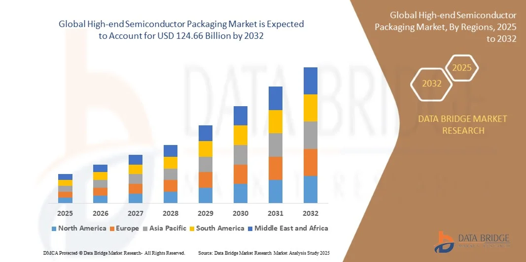
Global High End Semiconductor Packaging Market
Market Size in USD Billion
 USD
38.28 Billion
USD
124.66 Billion
2024
2032
USD
38.28 Billion
USD
124.66 Billion
2024
2032
| 2025 - 2032 | |
| USD 38.28 Billion | |
| USD 124.66 Billion | |
| % | |
|
What is the Global High-end Semiconductor Packaging Market Size and Growth Rate?
- The global high-end semiconductor packaging market size was valued at USD 38.28 billion in 2024 and is expected to reach USD 124.66 billion by 2032, at a CAGR of 15.9% during the forecast period
- High-end semiconductor packaging technologies, including 3D packaging, fan-out wafer-level packaging, and system-in-package solutions, are emerging as essential enablers for next-generation electronic devices by enhancing functionality, speed, and power efficiency
- The market’s momentum is fueled by growing demand in data centers, consumer electronics, automotive, and telecommunications, coupled with rapid digitalization and the adoption of high-performance computing solutions
What are the Major Takeaways of High-end Semiconductor Packaging Market?
- Market growth is primarily driven by the rising demand for advanced packaging solutions to support miniaturization, improved power efficiency, and higher performance across electronics, consumer devices, and industrial applications
- In addition, the increasing penetration of 5G, AI, IoT, and automotive electronics is creating substantial opportunities for innovative high-end packaging technologies, thereby accelerating the overall industry expansion
- North America dominated the high-end semiconductor packaging market with the largest revenue share of 35.69% in 2024, driven by strong demand for advanced electronics, telecommunication equipment, and automotive semiconductors
- The Asia-Pacific (APAC) market is poised to grow at the fastest CAGR of 9.14% from 2025 to 2032, fueled by rapid urbanization, technological advancements, and growing electronics manufacturing in China, Japan, South Korea, and India
- The consumer electronics segment dominated the market with the largest revenue share of 42.3% in 2024, driven by the widespread adoption of smartphones, tablets, and wearables that demand compact, power-efficient, and high-performance chips
Report Scope and High-end Semiconductor Packaging Market Segmentation
|
Attributes |
High-end Semiconductor Packaging Key Market Insights |
|
Segments Covered |
|
|
Countries Covered |
North America
Europe
Asia-Pacific
Middle East and Africa
South America
|
|
Key Market Players |
|
|
Market Opportunities |
|
|
Value Added Data Infosets |
In addition to the insights on market scenarios such as market value, growth rate, segmentation, geographical coverage, and major players, the market reports curated by the Data Bridge Market Research also include in-depth expert analysis, pricing analysis, brand share analysis, consumer survey, demography analysis, supply chain analysis, value chain analysis, raw material/consumables overview, vendor selection criteria, PESTLE Analysis, Porter Analysis, and regulatory framework. |
What is the Key Trend in the High-end Semiconductor Packaging Market?
Integration of Advanced Packaging with AI and Heterogeneous Computing
- A defining trend in the global high-end semiconductor packaging market is the rapid integration of artificial intelligence (AI) and heterogeneous computing architectures within packaging technologies. Advanced approaches such as 2.5D, 3D IC packaging, fan-out wafer-level packaging (FOWLP), and system-in-package (SiP) are enabling higher performance, lower latency, and energy-efficient designs tailored for AI and high-performance computing (HPC)
- For instance, TSMC’s CoWoS (Chip-on-Wafer-on-Substrate) packaging technology is widely adopted in AI accelerators, providing seamless integration of high-bandwidth memory (HBM) with logic dies, significantly boosting data throughput. Similarly, Intel’s Foveros 3D packaging allows vertical stacking of dies, improving performance density and efficiency for advanced computing
- AI-driven design and simulation tools are also being integrated into semiconductor packaging processes, enabling smarter routing, yield optimization, and predictive failure analysis. Companies are increasingly leveraging machine learning algorithms to enhance manufacturing efficiency, defect detection, and lifecycle management of advanced packages
- The rise of chiplet-based designs is further accelerating demand for advanced packaging. Leading firms such as AMD and Intel are adopting chiplet integration using advanced interconnect technologies such as EMIB (Embedded Multi-Die Interconnect Bridge) and hybrid bonding to deliver scalable performance while reducing costs
- This shift towards AI-optimized, heterogeneous, and chiplet-compatible packaging is redefining industry standards. Consequently, global players are investing heavily in R&D to remain competitive, as advanced packaging becomes a critical enabler for next-generation AI, 5G, and edge computing markets
- The demand for AI- and HPC-ready semiconductor packaging solutions is rapidly expanding across data centers, consumer electronics, and automotive applications, positioning this trend as a central driver of market transformation
What are the Key Drivers of High-end Semiconductor Packaging Market?
- The surging demand for AI, IoT, 5G, and automotive electronics is a primary driver, as these technologies require advanced packaging to meet performance, size, and power efficiency requirements
- For instance, in 2024, Amkor Technology expanded its advanced packaging facility in Vietnam, aimed at supporting the growing demand for automotive and AI chip packaging solutions, highlighting the industry’s growth trajectory
- Increasing adoption of fan-out wafer-level packaging (FOWLP), through-silicon via (TSV), and hybrid bonding technologies enables smaller form factors, enhanced performance, and better power management, fueling market growth
- Moreover, the proliferation of edge devices, wearables, and miniaturized consumer electronics is boosting demand for high-end packaging that supports compact yet powerful chip architectures
- Another driver is the shift towards system-in-package (SiP) solutions, which integrate multiple functions into a single module, enabling faster time-to-market and reduced overall system costs for manufacturers
- Collectively, these factors are strengthening the role of high-end packaging as a core enabler of next-gen semiconductor innovation, particularly in HPC, AI, 5G networks, and automotive electronics
Which Factor is Challenging the Growth of the High-end Semiconductor Packaging Market?
- A major challenge lies in the high manufacturing cost and technical complexity of advanced semiconductor packaging solutions such as 2.5D/3D integration, TSV, and heterogeneous integration. The precision required in aligning multiple dies and ensuring reliable interconnectivity drives up production costs and yields variability
- For instance, 3D IC packaging using TSV technology involves high capital investments and faces thermal management issues, limiting its mass adoption in cost-sensitive markets
- Another critical barrier is the supply chain dependency on specialized materials such as advanced substrates, RDL (redistribution layers), and high-bandwidth memory (HBM), which remain concentrated among a few global suppliers, creating bottlenecks
- In addition, the longer qualification cycles required for automotive and aerospace applications can delay adoption timelines of new packaging innovations
- While market leaders such as ASE, Amkor, and JCET are investing in scaling technologies and automation to reduce costs, the premium pricing of high-end packaging still restricts adoption in emerging economies and for low-cost consumer devices
- Overcoming these challenges through scalable design platforms, material innovation, and cost-optimized packaging processes will be critical to ensuring sustainable market growth over the forecast period
How is the High-end Semiconductor Packaging Market Segmented?
The market is segmented on the basis of type, communication protocol, unlocking mechanism, and application.
- By Application
On the basis of application, the high-end semiconductor packaging market is segmented into consumer electronics, telecommunications, automotive, industrial electronics, and healthcare. The consumer electronics segment dominated the market with the largest revenue share of 42.3% in 2024, driven by the widespread adoption of smartphones, tablets, and wearables that demand compact, power-efficient, and high-performance chips. The increasing penetration of IoT-enabled devices and high-performance computing also reinforces packaging needs in this sector.
Meanwhile, the automotive segment is expected to witness the fastest CAGR of 17.6% from 2025 to 2032, fueled by the surge in electric vehicles (EVs), autonomous driving systems, and advanced driver-assistance systems (ADAS). Automotive OEMs are investing in packaging solutions that ensure reliability under harsh conditions while meeting miniaturization and efficiency demands. The growing convergence of connectivity, infotainment, and electrification technologies continues to push semiconductor packaging innovation across applications.
- By Type of Packaging
On the basis of type of packaging, the market is segmented into system in package (SiP), flip chip, ball grid array (BGA), chip on board (CoB), and 3D packaging. The flip chip segment captured the largest market share of 36.4% in 2024, attributed to its superior electrical performance, reduced signal delay, and widespread use in consumer electronics and data centers. Flip chip packaging is also favored for enabling higher input/output density and efficient heat dissipation.
However, the 3D packaging segment is projected to grow at the fastest CAGR of 19.2% from 2025 to 2032, as it facilitates stacking of multiple dies, reduces form factor, and enhances system performance. The increasing need for high-bandwidth memory (HBM) in AI, 5G, and HPC applications is driving strong demand for 3D integration. This shift underscores the industry’s transition toward advanced miniaturization and performance-driven designs.
- By Material
On the basis of material, the high-end semiconductor packaging market is segmented into silicon, ceramics, glass, polymers, and metals. The silicon segment dominated the market with the largest revenue share of 48.1% in 2024, as it remains the fundamental substrate material for advanced packaging due to its excellent thermal conductivity, electrical performance, and scalability. Silicon interposers are extensively used in 2.5D and 3D packaging applications to enhance signal integrity and bandwidth.
On the other hand, the glass segment is anticipated to grow at the fastest CAGR of 18.8% from 2025 to 2032, owing to its superior dimensional stability, low dielectric constant, and potential in next-generation fan-out wafer-level packaging and panel-level packaging. Glass substrates are being increasingly researched and commercialized for high-frequency applications, especially in 5G and advanced RF devices, signaling their role as a disruptive material in the packaging landscape.
- By End-Use Industry
On the basis of end-use industry, the market is segmented into telecommunication, automotive, aerospace, medical, and consumer electronics. The telecommunication segment accounted for the largest revenue share of 39.6% in 2024, driven by the rapid rollout of 5G infrastructure, the rising demand for high-performance networking equipment, and increasing deployment of cloud computing and data centers. Advanced packaging technologies such as SiP and 2.5D integration are widely deployed to enhance signal speed and reduce power consumption in telecom applications.
Conversely, the aerospace segment is forecasted to expand at the fastest CAGR of 17.1% from 2025 to 2032, driven by growing reliance on advanced electronics in satellite communication, avionics, and defense applications. Aerospace packaging emphasizes durability, reliability, and resistance to extreme conditions, pushing innovation in high-reliability semiconductor packaging solutions tailored for critical missions.
Which Region Holds the Largest Share of the High-end Semiconductor Packaging Market?
- North America dominated the high-end semiconductor packaging market with the largest revenue share of 35.69% in 2024, driven by strong demand for advanced electronics, telecommunication equipment, and automotive semiconductors
- Companies and consumers in the region highly value reliable, high-performance, and miniaturized semiconductor packaging solutions that enhance device efficiency, thermal management, and connectivity
- This widespread adoption is further supported by robust industrial infrastructure, technological innovation hubs, and high R&D investments, establishing North America as a leader in advanced semiconductor packaging solutions
U.S. High-end Semiconductor Packaging Market Insight
The U.S. high-end semiconductor packaging market captured the largest revenue share of 81% in North America in 2024, fueled by the rapid adoption of high-performance computing, 5G infrastructure, and consumer electronics. The growing integration of AI, IoT devices, and EV electronics drives demand for compact and reliable packaging. Increasing R&D initiatives, along with government support for advanced semiconductor manufacturing, are significantly expanding the market footprint in the country.
Europe High-end Semiconductor Packaging Market Insight
The Europe market is expected to expand at a substantial CAGR, driven by growing demand in automotive electronics, industrial automation, and telecommunication systems. Regulatory emphasis on energy-efficient electronics and stringent quality standards is promoting adoption of high-reliability packaging solutions. Countries such as Germany, France, and Italy are witnessing significant growth across both consumer and industrial applications.
U.K. High-end Semiconductor Packaging Market Insight
The U.K. market is anticipated to grow at a notable CAGR during the forecast period, supported by increased adoption of telecommunications infrastructure, electric vehicles, and consumer electronics. The presence of leading semiconductor R&D centers and investments in smart manufacturing technologies continues to foster market growth.
Germany High-end Semiconductor Packaging Market Insight
Germany’s market is projected to grow considerably, driven by advanced automotive electronics, industrial automation, and aerospace applications. Germany’s emphasis on sustainable and energy-efficient electronic solutions promotes high-end semiconductor packaging adoption, with a focus on thermal management, miniaturization, and reliability.
Which Region is the Fastest Growing Region in the High-end Semiconductor Packaging Market?
The Asia-Pacific (APAC) market is poised to grow at the fastest CAGR of 9.14% from 2025 to 2032, fueled by rapid urbanization, technological advancements, and growing electronics manufacturing in China, Japan, South Korea, and India. Rising adoption of EVs, 5G, IoT devices, and consumer electronics is driving demand. Government initiatives to strengthen semiconductor manufacturing and the availability of cost-effective components are further expanding market penetration.
Japan High-end Semiconductor Packaging Market Insight
Japan’s market is growing steadily due to its high-tech culture, extensive electronics industry, and increasing adoption of advanced semiconductor packaging in automotive, robotics, and consumer electronics. Demand for high-reliability packaging solutions in industrial and consumer sectors continues to expand.
China High-end Semiconductor Packaging Market Insight
China accounted for the largest market revenue share in APAC in 2024, driven by the country’s massive consumer electronics market, growing EV industry, and expanding semiconductor manufacturing ecosystem. Domestic investment in smart devices, high-performance computing, and telecom infrastructure is fueling adoption of advanced packaging solutions.
Which are the Top Companies in High-end Semiconductor Packaging Market?
The high-end semiconductor packaging industry is primarily led by well-established companies, including:
- ASE Technology Holding Co., Ltd. (Taiwan)
- Amkor Technology, Inc. (U.S.)
- JCET Group Co., Ltd. (China)
- Siliconware Precision Industries Co. Ltd. (Taiwan)
- Powertech Technology Inc. (Taiwan)
- Tianshui Huatian Technology Co. Ltd. (China)
- Fujitsu Semiconductor Ltd. (Japan)
- UTAC (Singapore)
- ChipMOS TECHNOLOGIES INC. (Taiwan)
- CHIPBOND Technology Corporation (Taiwan)
- Intel Corporation (U.S.)
- Samsung Electronics Co., Ltd. (South Korea)
- Unisem (M) Berhad (Malaysia)
- Camtek Ltd. (Israel)
- LG Chem Ltd. (South Korea)
What are the Recent Developments in Global High-end Semiconductor Packaging Market?
- In March 2024, the U.S. Department of Commerce and Intel Corporation entered into a non-binding preliminary memorandum of terms (PMT), under which Intel will receive USD 8.5 billion in direct funding for its commercial semiconductor projects under the CHIPS and Science Act. This initiative is expected to significantly accelerate semiconductor packaging demand across the U.S. market
- In March 2024, Taiwan Semiconductor Manufacturing Company Limited announced plans to build an advanced packaging facility in Japan, introducing its chip-on-wafer-on-substrate (CoWoS) packaging technology, which involves stacking chips vertically to enhance processing power and reduce energy use. This strategic move is set to strengthen Japan’s position in advanced semiconductor packaging
- In November 2023, JCET Automotive Electronics (Shanghai) Co., Ltd., a subsidiary of Jiangsu Changdian Technology Co., Ltd., secured an investment of USD 0.60 billion (CNY 4.4 billion) to establish an advanced packaging facility for automotive chip products in the Lingang Special Area of Shanghai. This investment will expand JCET’s capabilities in catering to the rising demand for automotive semiconductors
- In September 2023, Intel Corporation launched a glass substrate designed for next-generation advanced packaging, offering superior mechanical and thermal stability, along with ultra-low flatness that enhances interconnect density in substrates. This innovation is anticipated to boost the production of high-performance, high-density chip packages for data-intensive workloads
SKU-
- Interactive Data Analysis Dashboard
- Company Analysis Dashboard for high growth potential opportunities
- Research Analyst Access for customization & queries
- Competitor Analysis with Interactive dashboard
- Latest News, Updates & Trend analysis
- Harness the Power of Benchmark Analysis for Comprehensive Competitor Tracking
Global High End Semiconductor Packaging Market, Supply Chain Analysis and Ecosystem Framework
To support market growth and help clients navigate the impact of geopolitical shifts, DBMR has integrated in-depth supply chain analysis into its Global High End Semiconductor Packaging Market research reports. This addition empowers clients to respond effectively to global changes affecting their industries. The supply chain analysis section includes detailed insights such as Global High End Semiconductor Packaging Market consumption and production by country, price trend analysis, the impact of tariffs and geopolitical developments, and import and export trends by country and HSN code. It also highlights major suppliers with data on production capacity and company profiles, as well as key importers and exporters. In addition to research, DBMR offers specialized supply chain consulting services backed by over a decade of experience, providing solutions like supplier discovery, supplier risk assessment, price trend analysis, impact evaluation of inflation and trade route changes, and comprehensive market trend analysis.
Data collection and base year analysis are done using data collection modules with large sample sizes. The stage includes obtaining market information or related data through various sources and strategies. It includes examining and planning all the data acquired from the past in advance. It likewise envelops the examination of information inconsistencies seen across different information sources. The market data is analysed and estimated using market statistical and coherent models. Also, market share analysis and key trend analysis are the major success factors in the market report. To know more, please request an analyst call or drop down your inquiry.
The key research methodology used by DBMR research team is data triangulation which involves data mining, analysis of the impact of data variables on the market and primary (industry expert) validation. Data models include Vendor Positioning Grid, Market Time Line Analysis, Market Overview and Guide, Company Positioning Grid, Patent Analysis, Pricing Analysis, Company Market Share Analysis, Standards of Measurement, Global versus Regional and Vendor Share Analysis. To know more about the research methodology, drop in an inquiry to speak to our industry experts.
Data Bridge Market Research is a leader in advanced formative research. We take pride in servicing our existing and new customers with data and analysis that match and suits their goal. The report can be customized to include price trend analysis of target brands understanding the market for additional countries (ask for the list of countries), clinical trial results data, literature review, refurbished market and product base analysis. Market analysis of target competitors can be analyzed from technology-based analysis to market portfolio strategies. We can add as many competitors that you require data about in the format and data style you are looking for. Our team of analysts can also provide you data in crude raw excel files pivot tables (Fact book) or can assist you in creating presentations from the data sets available in the report.


