
Global Non Uv Dicing Tape Market
Market Size in USD Billion
 USD
152.45 Billion
USD
246.67 Billion
2025
2033
USD
152.45 Billion
USD
246.67 Billion
2025
2033
| 2026 - 2033 | |
| USD 152.45 Billion | |
| USD 246.67 Billion | |
| % | |
|
Non-Ultraviolet (UV) Dicing Tape Market Overview
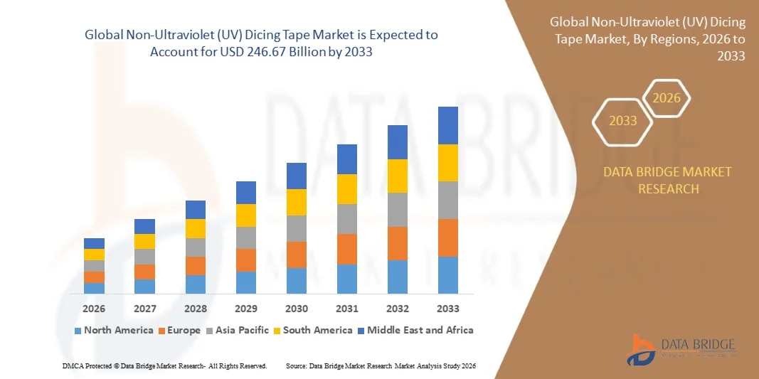
The Non-Ultraviolet (UV) Dicing Tape Market was valued at USD 152.45 billion in 2025 and is projected to reach USD 246.67 billion by 2033, growing at a CAGR of 6.20% from 2026 to 2033. The market is witnessing steady growth driven by rising demand for advanced semiconductor packaging solutions, increasing wafer-level processing in electronics manufacturing, and expanding applications across consumer electronics, automotive semiconductors, and industrial devices.
The growing miniaturization of electronic components, combined with the rapid expansion of semiconductor fabrication facilities globally, is encouraging the adoption of non-UV dicing tapes due to their cost efficiency, strong adhesion performance, and suitability for high-volume wafer dicing processes. In addition, increasing investments in 5G infrastructure, artificial intelligence hardware, and advanced computing systems are further accelerating demand for high-precision dicing materials in semiconductor manufacturing.
Key Market Trends & Insights
- North America dominated the non-ultraviolet (UV) dicing tape market with the largest revenue share of approximately 34.9% in 2025, supported by strong semiconductor manufacturing activity, advanced packaging technologies, and increasing demand for high-performance electronics. The region benefits from well-established semiconductor fabs, high adoption of AI-driven computing hardware, and continuous investment in wafer-level packaging technologies.
- Asia-Pacific is expected to be the fastest-growing region, recording a CAGR of 7.4% from 2026 to 2033. Growth is driven by large-scale semiconductor production, rapid expansion of electronics manufacturing hubs, and increasing investments in advanced packaging technologies across countries such as China, Japan, South Korea, and Taiwan.
- The PET segment held the largest market revenue share of approximately 58.4% in 2025 driven by its superior dimensional stability, high thermal resistance, and excellent adhesion performance during wafer dicing processes. PET-based tapes are widely used in advanced semiconductor packaging due to their ability to minimize wafer deformation and maintain structural integrity during high-speed precision cutting.
- The PO segment is projected to register the fastest growth at a CAGR of 9.6% from 2026 to 2033, driven by increasing adoption in ultra-thin wafer processing and next-generation semiconductor devices. Growing demand for flexible and low-stress adhesive materials in advanced packaging applications is accelerating segment expansion across high-performance chip manufacturing facilities.
- The 85–125 Micron segment held the largest market revenue share of approximately 44.7% in 2025 driven by its balanced mechanical strength and flexibility, making it suitable for standard wafer dicing operations in consumer electronics and semiconductor fabrication. This thickness range is widely preferred for stable handling of silicon wafers during precision cutting processes.
- The Below 85 Micron segment is projected to register the fastest growth at a CAGR of 10.2% from 2026 to 2033, driven by rising demand for ultra-thin wafers used in advanced semiconductor miniaturization, AI chips, and 5G devices. Increasing focus on high-density chip architectures is further supporting adoption of thinner dicing tape solutions.
- The Single Sided segment held the largest market revenue share of approximately 67.9% in 2025 driven by its extensive use in wafer dicing applications where secure adhesion to a single surface is required during cutting and die separation processes. Single sided tapes are widely adopted due to their ease of handling and cost efficiency in high-volume semiconductor manufacturing.
- The Double Sided segment is projected to register the fastest growth at a CAGR of 8.8% from 2026 to 2033, driven by increasing demand in advanced packaging applications where temporary bonding and multi-layer wafer processing are required. Rising adoption in fan-out wafer-level packaging and system-in-package technologies is accelerating segment growth.
- The Wafer Dicing segment held the largest market revenue share of approximately 72.5% in 2025 driven by extensive use in semiconductor wafer slicing processes across memory chips, logic ICs, and power semiconductor devices. Wafer dicing remains a critical step in semiconductor manufacturing, requiring high-precision adhesive materials to minimize chip breakage and improve yield efficiency.
- The Package Dicing segment is projected to register the fastest growth at a CAGR of 9.3% from 2026 to 2033, driven by increasing adoption of advanced semiconductor packaging technologies such as 3D ICs and wafer-level packaging. Growing demand for high-performance computing, AI processors, and compact electronic devices is further accelerating segment expansion in this category.
Market Size & Forecast
- Global Market Value (2025): USD 152.45 Billion
- Expected Market Value (2033): USD 246.67 Billion
- Forecast CAGR (2026–2033): 6.20%
- Leading Region in 2025: North America
- Fastest Growing Region: Asia-Pacific
Report Scope and Non-Ultraviolet (UV) Dicing Tape Market Segmentation
|
Attributes |
Non-Ultraviolet (UV) Dicing Tape Key Market Insights |
|
Segments Covered |
· By Material Type: PVC (Polyvinyl Chloride), PET (Polyethylene Terephthalate), PO, and Others · By Thickness: 85-125 Micron, 126-150 Micron, Below 85 Micron, and Above 150 Micron · By Coating Type: Single Sided and Double Sided · By Application: Wafer Dicing, Package Dicing, and Others |
|
Countries Covered |
North America · U.S. · Canada · Mexico Europe · Germany · France · U.K. · Netherlands · Switzerland · Belgium · Russia · Italy · Spain · Turkey · Rest of Europe Asia-Pacific · China · Japan · India · South Korea · Singapore · Malaysia · Australia · Thailand · Indonesia · Philippines · Rest of Asia-Pacific Middle East and Africa · Saudi Arabia · U.A.E. · South Africa · Egypt · Israel · Rest of Middle East and Africa South America · Brazil · Argentina · Rest of South America |
|
Key Market Players |
• Mitsui Chemicals, Inc. (Japan) |
|
Market Opportunities |
|
|
Value Added Data Infosets |
In addition to the insights on market scenarios such as market value, growth rate, segmentation, geographical coverage, and major players, the market reports curated by the Data Bridge Market Research also include import export analysis, production capacity overview, production consumption analysis, price trend analysis, climate change scenario, supply chain analysis, value chain analysis, raw material/consumables overview, vendor selection criteria, PESTLE Analysis, Porter Analysis, and regulatory framework. |
Non-Ultraviolet (UV) Dicing Tape Market Trends
Trend: Growth In Advanced Semiconductor Packaging And High-Precision Wafer Dicing Applications
Increasing demand for high-reliability, contamination-free, and mechanically stable wafer processing materials across semiconductor manufacturing and electronics assembly sectors. Conventional dicing support materials often face challenges in adhesion stability, residue control, and wafer integrity during high-speed slicing processes, encouraging manufacturers to adopt non-ultraviolet (UV) dicing tapes for improved process efficiency and yield performance.
In modern semiconductor fabrication, non-UV dicing tapes are widely used during wafer dicing and die-attach processes, For instance in memory chips, logic ICs, and power semiconductor devices, to ensure stable wafer holding strength and reduced chip damage during high-precision cutting operations. In advanced packaging facilities, these tapes are increasingly utilized in wafer-level packaging (WLP) and system-in-package (SiP) technologies to enhance structural stability and improve production throughput.
The rapid expansion of consumer electronics, electric vehicles, and high-performance computing infrastructure is also increasing demand for ultra-thin wafers and defect-free dicing processes capable of supporting miniaturized chip architectures. In addition, semiconductor foundries continue to rely on high-performance dicing materials in AI chips and 5G-enabled devices, such as those produced in Taiwan and South Korea, due to their ability to maintain wafer integrity during extreme precision cutting processes. Growing industry validation through 2025 semiconductor pilot production lines integrating next-generation dicing tapes is showing yield improvements of nearly 6–10% in wafer breakage reduction and die placement accuracy optimization.
Non-Ultraviolet (UV) Dicing Tape Market Dynamics
Key Market Driver: Rising Demand For Advanced Semiconductor Manufacturing And Yield Optimization
Industries worldwide are facing increasing demand for higher chip performance, miniaturization, and production efficiency, driving strong adoption of advanced wafer dicing materials. Rapid growth in semiconductor applications across automotive electronics, consumer devices, and industrial automation is increasing the need for stable and contamination-free dicing solutions.
Semiconductor manufacturers are increasingly deploying non-UV dicing tapes to improve wafer handling efficiency and reduce mechanical stress during dicing processes. For instance, leading foundries in Taiwan and South Korea are adopting advanced tape solutions in 300 mm wafer production lines to minimize die chipping and improve yield rates in high-volume manufacturing environments.
Similarly, expansion of AI chip production and 5G device manufacturing is driving demand for high-precision wafer processing materials. Real-world semiconductor fab implementations in 2024 across Japan and South Korea reported wafer damage reduction of around 5–8% after transitioning to advanced non-UV dicing tape solutions in high-speed dicing operations.
Key Restraint/Challenge: Performance Limitations And Process Sensitivity In Extreme Fabrication Conditions
Non-UV dicing tapes face limitations in extreme thermal and mechanical conditions during advanced semiconductor processing, which can affect adhesion performance and wafer stability. Variations in temperature, humidity, and processing speed can influence tape behavior, creating challenges in achieving consistent results across different fabrication environments.
In addition, high dependency on precision manufacturing environments increases operational complexity and limits flexibility for small-scale semiconductor producers. Compatibility issues with ultra-thin wafers and next-generation chip architectures also restrict widespread adoption in certain advanced packaging applications.
Commercial benchmarking studies indicate that wafer breakage rates during dicing operations can vary between 3–7% depending on tape quality and process conditions, making process optimization a critical requirement for maintaining high production yields in advanced semiconductor fabs.
Key Market Opportunity: Expansion Of AI, 5G, And Advanced Packaging Semiconductor Ecosystem
Modern AI processors, 5G chipsets, automotive semiconductors, and IoT devices increasingly require high-density, low-defect wafer processing solutions. Growing complexity in semiconductor architectures is creating strong demand for advanced dicing tapes capable of supporting ultra-thin wafer handling and multi-layer packaging technologies.
Semiconductor companies are increasingly adopting non-UV dicing tapes in advanced packaging processes, For instance in fan-out wafer-level packaging and 3D IC integration, to improve structural stability and reduce wafer damage during die separation. In AI hardware manufacturing, rising chip density and heat sensitivity are further driving demand for high-performance dicing materials.
In addition, advancements in adhesive chemistry and polymer engineering are improving tape performance, opening opportunities across semiconductor fabs in Asia-Pacific and North America. Semiconductor production expansions in 2025 across Taiwan, South Korea, and the U.S. are reporting improved yield efficiency of around 6–9% after integrating next-generation non-UV dicing tape technologies in high-volume manufacturing lines.
Non-Ultraviolet (UV) Dicing Tape Market Scope
The market is segmented on the basis of material type, thickness, coating type, and application.
- By Material Type
On the basis of material type, the non-ultraviolet (UV) dicing tape market is segmented into PVC (Polyvinyl Chloride), PET (Polyethylene Terephthalate), PO, and Others. The PET segment held the largest market revenue share of approximately 58.4% in 2025 driven by its superior dimensional stability, high thermal resistance, and excellent adhesion performance during wafer dicing processes. PET-based tapes are widely used in advanced semiconductor packaging due to their ability to minimize wafer deformation and maintain structural integrity during high-speed precision cutting.
The PO segment is projected to register the fastest growth at a CAGR of 9.6% from 2026 to 2033, driven by increasing adoption in ultra-thin wafer processing and next-generation semiconductor devices. Growing demand for flexible and low-stress adhesive materials in advanced packaging applications is accelerating segment expansion across high-performance chip manufacturing facilities.
- By Thickness
On the basis of thickness, the market is segmented into 85–125 Micron, 126–150 Micron, Below 85 Micron, and Above 150 Micron. The 85–125 Micron segment held the largest market revenue share of approximately 44.7% in 2025 driven by its balanced mechanical strength and flexibility, making it suitable for standard wafer dicing operations in consumer electronics and semiconductor fabrication. This thickness range is widely preferred for stable handling of silicon wafers during precision cutting processes.
The Below 85 Micron segment is projected to register the fastest growth at a CAGR of 10.2% from 2026 to 2033, driven by rising demand for ultra-thin wafers used in advanced semiconductor miniaturization, AI chips, and 5G devices. Increasing focus on high-density chip architectures is further supporting adoption of thinner dicing tape solutions.
- By Coating Type
On the basis of coating type, the market is segmented into Single Sided and Double Sided. The Single Sided segment held the largest market revenue share of approximately 67.9% in 2025 driven by its extensive use in wafer dicing applications where secure adhesion to a single surface is required during cutting and die separation processes. Single sided tapes are widely adopted due to their ease of handling and cost efficiency in high-volume semiconductor manufacturing.
The Double Sided segment is projected to register the fastest growth at a CAGR of 8.8% from 2026 to 2033, driven by increasing demand in advanced packaging applications where temporary bonding and multi-layer wafer processing are required. Rising adoption in fan-out wafer-level packaging and system-in-package technologies is accelerating segment growth.
- By Application
On the basis of application, the market is segmented into Wafer Dicing, Package Dicing, and Others. The Wafer Dicing segment held the largest market revenue share of approximately 72.5% in 2025 driven by extensive use in semiconductor wafer slicing processes across memory chips, logic ICs, and power semiconductor devices. Wafer dicing remains a critical step in semiconductor manufacturing, requiring high-precision adhesive materials to minimize chip breakage and improve yield efficiency.
The Package Dicing segment is projected to register the fastest growth at a CAGR of 9.3% from 2026 to 2033, driven by increasing adoption of advanced semiconductor packaging technologies such as 3D ICs and wafer-level packaging. Growing demand for high-performance computing, AI processors, and compact electronic devices is further accelerating segment expansion in this category.
Non-Ultraviolet (UV) Dicing Tape Market Regional Analysis
North America Non-Ultraviolet (UV) Dicing Tape Market Insight
North America dominated the non-ultraviolet (UV) dicing tape market with the largest revenue share of approximately 34.9% in 2025, supported by strong semiconductor manufacturing activity, advanced packaging technologies, and increasing demand for high-performance electronics. The region benefits from well-established semiconductor fabs, high adoption of AI-driven computing hardware, and continuous investment in wafer-level packaging technologies. Growing demand for miniaturized electronic components and advanced chip architectures is further strengthening market growth across consumer electronics, automotive, and industrial applications. The presence of leading semiconductor companies and advanced R&D infrastructure further enhances regional dominance in high-precision wafer processing materials.
U.S. Non-Ultraviolet (UV) Dicing Tape Market Insight
The U.S. non-ultraviolet (UV) dicing tape market captured the largest revenue share of approximately 29.7% in 2025 within North America, driven by rapid expansion of semiconductor fabrication facilities and increasing adoption of advanced packaging technologies for AI, 5G, and automotive electronics. Strong presence of leading semiconductor companies and continuous R&D investment in chip miniaturization are further supporting market growth. Rising demand for high-yield wafer processing and precision dicing materials is accelerating adoption across advanced semiconductor production lines. Increasing use of non-UV dicing tapes in memory chips, logic devices, and power semiconductors is further strengthening market expansion. Government initiatives supporting domestic semiconductor manufacturing are also contributing to sustained growth in the U.S. market.
Europe Non-Ultraviolet (UV) Dicing Tape Market Insight
The Europe non-ultraviolet (UV) dicing tape market is expected to witness the fastest growth rate from 2026 to 2033, primarily driven by increasing investments in semiconductor manufacturing, automotive electronics, and industrial automation technologies. The region’s strong focus on advanced chip design, energy-efficient electronics, and sustainable manufacturing practices is supporting market expansion. Growing demand for high-precision wafer processing in automotive semiconductor applications and industrial control systems is further accelerating adoption. Europe’s emphasis on technological sovereignty in semiconductor production is also encouraging investments in advanced packaging and dicing material solutions.
U.K. Non-Ultraviolet (UV) Dicing Tape Market Insight
The U.K. non-ultraviolet (UV) dicing tape market is expected to witness steady growth from 2026 to 2033, driven by increasing semiconductor R&D activities and expanding demand for advanced electronics in aerospace, defense, and telecommunications sectors. Rising focus on AI hardware development and high-performance computing systems is further supporting market growth. Growing investments in chip design and semiconductor innovation hubs are contributing to increased adoption of precision wafer dicing materials. The expansion of tech-driven manufacturing ecosystems is further strengthening demand for advanced dicing tape solutions.
Germany Non-Ultraviolet (UV) Dicing Tape Market Insight
The Germany non-ultraviolet (UV) dicing tape market is expected to witness strong growth from 2026 to 2033, fueled by the country’s advanced automotive semiconductor industry and strong industrial electronics base. Germany’s emphasis on precision engineering and high-reliability electronic components is supporting demand for advanced wafer processing materials. Increasing adoption of electric vehicles and industrial automation systems is further driving semiconductor demand. Integration of advanced packaging technologies in automotive and industrial chip manufacturing is strengthening the need for high-performance dicing tapes.
Asia-Pacific Non-Ultraviolet (UV) Dicing Tape Market Insight
The Asia-Pacific non-ultraviolet (UV) dicing tape market is expected to witness the fastest growth rate from 2026 to 2033, supported by large-scale semiconductor manufacturing in countries such as China, Japan, South Korea, and Taiwan. The region dominates global chip production, driving strong demand for wafer processing materials. Rapid expansion of consumer electronics, AI chips, and 5G infrastructure is further accelerating market growth. Increasing investments in semiconductor fabs and government initiatives promoting domestic chip manufacturing are also strengthening regional demand. Asia-Pacific remains a key hub for advanced packaging and wafer dicing operations.
Japan Non-Ultraviolet (UV) Dicing Tape Market Insight
The Japan non-ultraviolet (UV) dicing tape market is expected to witness steady growth from 2026 to 2033 due to the country’s strong semiconductor manufacturing ecosystem and high demand for precision electronics. Japan’s leadership in advanced materials and semiconductor equipment is supporting adoption of high-performance dicing tapes. Increasing focus on AI hardware, automotive electronics, and industrial automation is further driving demand. Strong integration of advanced packaging technologies in domestic semiconductor production is also contributing to market expansion.
China Non-Ultraviolet (UV) Dicing Tape Market Insight
The China non-ultraviolet (UV) dicing tape market accounted for the largest revenue share in Asia-Pacific in 2025, driven by massive semiconductor production capacity, rapid industrialization, and strong demand for consumer electronics. China’s dominance in electronics manufacturing is significantly supporting wafer processing material consumption. Government initiatives promoting semiconductor self-sufficiency and expansion of domestic fabrication facilities are further accelerating market growth. Increasing production of AI chips, 5G devices, and automotive semiconductors is strengthening demand for advanced dicing tape solutions across the country.
Non-Ultraviolet (UV) Dicing Tape Market Share
The Non-Ultraviolet (UV) Dicing Tape industry is primarily led by well-established companies, including:
• Mitsui Chemicals, Inc. (Japan)
• QES GROUP BERHAD (Malaysia)
• Pantech Tape Co., Ltd. (South Korea)
• Furukawa Electric Co., Ltd. (Japan)
• AI Technology, Inc. (U.S.)
• LINTEC Corporation (Japan)
• Simac (Italy)
• Particles Plus, Inc. (U.S.)
• AMC CO., LTD. (South Korea)
• 3M (U.S.)
• Sumitomo Bakelite Co., Ltd. (Japan)
• Daest Coating India Pvt Ltd. (India)
• Denka Company Limited (Japan)
• Ultron Systems, Inc. (U.S.)
• Nitto Denko Corporation (Japan)
• Loadpoint (U.K.)
• Showa Denko Materials Co., Ltd. (Japan)
Latest Developments in Non-Ultraviolet (UV) Dicing Tape Market
- In June 2023, Nitto Denko Corporation introduced an eco-friendly non-ultraviolet (UV) dicing tape product aimed at improving thermal resistance and process stability during semiconductor wafer dicing operations. The development focuses on enhancing sustainability while maintaining high-performance adhesion properties required for advanced microelectronics manufacturing. The solution is designed to support efficient wafer processing under elevated temperature conditions in high-volume semiconductor fabrication environments. This innovation is expected to reduce material waste and improve operational efficiency in chip production lines. It also strengthens the adoption of environmentally sustainable consumables in semiconductor packaging, supporting the industry’s shift toward green manufacturing practices.
- In November 2023, LINTEC Corporation launched a high-adhesion non-ultraviolet (UV) dicing tape developed for precision semiconductor wafer processing applications. The product is designed to improve wafer stability and minimize micro-cracking during high-speed dicing operations in advanced semiconductor manufacturing. It enhances yield efficiency and ensures greater accuracy in microelectronics fabrication processes. The innovation is particularly beneficial for memory chips, logic devices, and advanced packaging applications requiring high structural integrity. It is expected to strengthen production reliability and support increasing demand for miniaturized and high-performance semiconductor components globally.
SKU-
- Interactive Data Analysis Dashboard
- Company Analysis Dashboard for high growth potential opportunities
- Research Analyst Access for customization & queries
- Competitor Analysis with Interactive dashboard
- Latest News, Updates & Trend analysis
- Harness the Power of Benchmark Analysis for Comprehensive Competitor Tracking
Global Non Uv Dicing Tape Market, Supply Chain Analysis and Ecosystem Framework
To support market growth and help clients navigate the impact of geopolitical shifts, DBMR has integrated in-depth supply chain analysis into its Global Non Uv Dicing Tape Market research reports. This addition empowers clients to respond effectively to global changes affecting their industries. The supply chain analysis section includes detailed insights such as Global Non Uv Dicing Tape Market consumption and production by country, price trend analysis, the impact of tariffs and geopolitical developments, and import and export trends by country and HSN code. It also highlights major suppliers with data on production capacity and company profiles, as well as key importers and exporters. In addition to research, DBMR offers specialized supply chain consulting services backed by over a decade of experience, providing solutions like supplier discovery, supplier risk assessment, price trend analysis, impact evaluation of inflation and trade route changes, and comprehensive market trend analysis.
Data collection and base year analysis are done using data collection modules with large sample sizes. The stage includes obtaining market information or related data through various sources and strategies. It includes examining and planning all the data acquired from the past in advance. It likewise envelops the examination of information inconsistencies seen across different information sources. The market data is analysed and estimated using market statistical and coherent models. Also, market share analysis and key trend analysis are the major success factors in the market report. To know more, please request an analyst call or drop down your inquiry.
The key research methodology used by DBMR research team is data triangulation which involves data mining, analysis of the impact of data variables on the market and primary (industry expert) validation. Data models include Vendor Positioning Grid, Market Time Line Analysis, Market Overview and Guide, Company Positioning Grid, Patent Analysis, Pricing Analysis, Company Market Share Analysis, Standards of Measurement, Global versus Regional and Vendor Share Analysis. To know more about the research methodology, drop in an inquiry to speak to our industry experts.
Data Bridge Market Research is a leader in advanced formative research. We take pride in servicing our existing and new customers with data and analysis that match and suits their goal. The report can be customized to include price trend analysis of target brands understanding the market for additional countries (ask for the list of countries), clinical trial results data, literature review, refurbished market and product base analysis. Market analysis of target competitors can be analyzed from technology-based analysis to market portfolio strategies. We can add as many competitors that you require data about in the format and data style you are looking for. Our team of analysts can also provide you data in crude raw excel files pivot tables (Fact book) or can assist you in creating presentations from the data sets available in the report.


