

What is the Global Photolithography Market Size and Growth Rate?
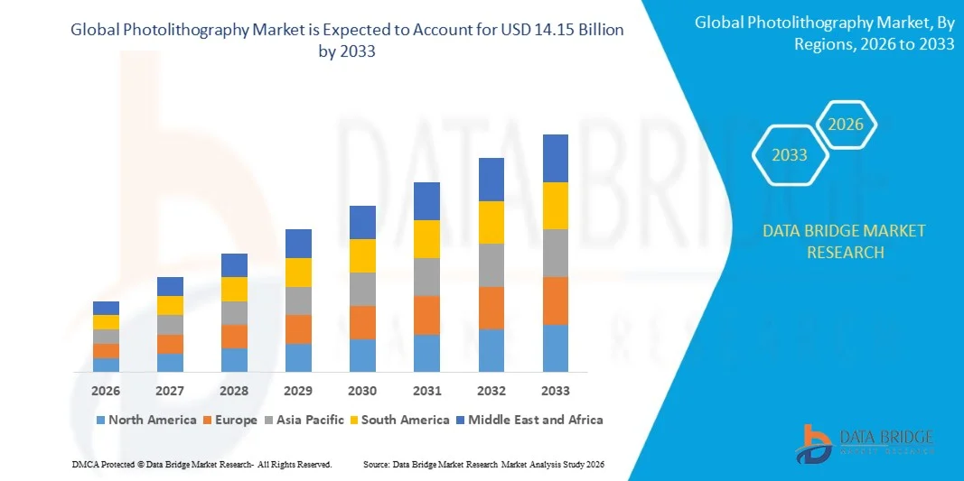
- As per Data Bridge Market Research Analysis the Global photolithography market size was valued at USD 10.26 billion in 2025 and is expected to reach USD 14.15 billion by 2033, at a CAGR of 4.10% during the forecast period
- The surging digitization and the emerging demand for semiconductor devices across various industries are the major factor responsible for driving the growth of market
- Moreover, the factors such as the increase in the production of computer chips, growing electronics packaging market and its advantages such as high resolution, high sensitivity to light, good adhesion properties and it allows 3D encapsulation of cells within hydrogels which fuels the growth of the photolithography market.
Market Size & Forecast
- Global Market Value (2025): USD 10.26 Billion
- Expected Market Value (2033): USD 14.15 Billion
- Forecast CAGR (2026–2033): 4.10%
What are the Major Takeaways of Photolithography Market?
- The advent of innovative and advanced technologies for semiconductor device manufacturing and increased government support for advancements is expected to create various new opportunities that will lead to the growth of the photolithography market in the above mentioned forecasted period
- The functional defects in the photolithography device, limited reliability of exposure tools and the complexities during the manufacturing procedure are estimated to pose as a major challenge hindering the growth of the photolithography market
- Asia-Pacific dominated the photolithography market with a 46.7% revenue share in 2025, driven by the strong presence of semiconductor manufacturing hubs, large-scale electronics production, and rapid expansion of advanced chip fabrication facilities across China, Taiwan, South Korea, and Japan
- North America is projected to register the fastest CAGR of 7.36% from 2026 to 2033, driven by increasing investments in semiconductor research, advanced chip design, and domestic fabrication initiatives across the U.S. and Canada
- The Deep Ultraviolet (DUV) segment dominated the market with a 41.6% share in 2025, as it remains the most widely used technology in semiconductor manufacturing for patterning integrated circuits at advanced and mature nodes
Report Scope and Photolithography Market Segmentation
|
Attributes |
Photolithography Key Market Insights |
|
Segments Covered |
|
|
Countries Covered |
North America
Europe
Asia-Pacific
Middle East and Africa
South America
|
|
Key Market Players |
|
|
Market Opportunities |
|
|
Value Added Data Infosets |
In addition to the insights on market scenarios such as market value, growth rate, segmentation, geographical coverage, and major players, the market reports curated by the Data Bridge Market Research also include in-depth expert analysis, pricing analysis, brand share analysis, consumer survey, demography analysis, supply chain analysis, value chain analysis, raw material/consumables overview, vendor selection criteria, PESTLE Analysis, Porter Analysis, and regulatory framework. |
What is the Key Trend in the Photolithography Market?
“Increasing Transition Toward Advanced EUV and High-Precision Photolithography Technologies”
- The photolithography market is witnessing strong adoption of Extreme Ultraviolet (EUV) lithography and advanced patterning technologies designed to support next-generation semiconductor fabrication and high-density chip architectures
- Equipment manufacturers are introducing high-precision exposure systems, improved alignment technologies, and advanced photoresist materials that enable smaller node sizes, improved pattern resolution, and higher wafer throughput
- Growing demand for high-performance processors, AI chips, advanced memory devices, and 5G communication components is accelerating the adoption of advanced lithography technologies across semiconductor fabrication facilities
- For instance, companies such as Canon, Nikon, Lam Research, and Samsung Electronics are expanding investments in next-generation lithography systems, advanced wafer processing technologies, and high-resolution semiconductor manufacturing solutions
- Increasing need for smaller transistor geometries, improved chip performance, and higher manufacturing precision is driving the transition toward advanced lithography techniques and multi-patterning technologies
- As semiconductor devices continue to scale down in size and increase in complexity, Photolithography technologies will remain essential for enabling next-generation semiconductor manufacturing and high-performance electronic devices
What are the Key Drivers of Photolithography Market?
- Rising demand for high-performance semiconductors, AI processors, advanced memory chips, and high-speed communication devices is significantly increasing the need for advanced photolithography systems in semiconductor fabrication
- For instance, in 2025, leading companies such as Canon, Nikon, and Lam Research expanded their semiconductor manufacturing equipment portfolios to support high-resolution lithography processes and next-generation chip fabrication technologies
- Growing adoption of 5G infrastructure, artificial intelligence, autonomous vehicles, consumer electronics, and cloud computing systems is accelerating semiconductor production globally across the U.S., Europe, and Asia-Pacific
- Advancements in EUV lithography, photoresist materials, wafer alignment technologies, and precision optical systems have improved manufacturing accuracy, throughput, and semiconductor yield rates
- Rising development of advanced semiconductor nodes, high-density integrated circuits, and high-speed computing architectures is creating strong demand for advanced photolithography equipment in modern semiconductor fabs
- Supported by increasing investments in semiconductor manufacturing capacity, government chip initiatives, and next-generation electronics innovation, the Photolithography market is expected to experience sustained long-term growth
Which Factor is Challenging the Growth of the Photolithography Market?
- High capital investment and operational costs associated with advanced photolithography equipment remain a major barrier for new semiconductor fabrication facilities and smaller chip manufacturers
- For instance, during 2024–2025, fluctuations in semiconductor supply chains, rising costs of precision optical components, and increasing equipment complexity raised manufacturing costs for several global semiconductor equipment vendors
- Complexity in implementing advanced lithography processes, EUV technologies, and multi-patterning techniques requires highly skilled engineers, specialized infrastructure, and extensive technical expertise
- Limited semiconductor fabrication infrastructure in emerging economies and high technological entry barriers slow the adoption of advanced photolithography systems in certain regions
- Competition from alternative chip manufacturing technologies, advanced packaging solutions, and evolving semiconductor design architectures may create technological and pricing pressures within the industry
- To address these challenges, companies are focusing on developing cost-efficient lithography systems, improving photoresist technologies, enhancing automation, and expanding global semiconductor manufacturing partnerships to accelerate the adoption of Photolithography technologies worldwide
How is the Photolithography Market Segmented?
The market is segmented on the basis of type, application, and end use.
• By Type
On the basis of type, the photolithography market is segmented into Deep Ultraviolet (DUV), Extreme Ultraviolet (EUV), I-line, Krypton Fluoride (KRF), Argon Fluoride Dry (ARF Dry), and Others. The Deep Ultraviolet (DUV) segment dominated the market with a 41.6% share in 2025, as it remains the most widely used technology in semiconductor manufacturing for patterning integrated circuits at advanced and mature nodes. DUV lithography systems offer high precision, reliability, and compatibility with large-scale semiconductor fabrication processes. They are extensively deployed in memory chips, logic devices, and microcontroller production due to their established infrastructure and cost-effectiveness compared with next-generation technologies.
The Extreme Ultraviolet (EUV) segment is expected to grow at the fastest CAGR from 2026 to 2033, driven by increasing demand for advanced semiconductor nodes below 7 nm. EUV technology enables the creation of smaller transistor structures, improving chip performance, energy efficiency, and processing speed. Rising investments in advanced foundries and next-generation chip manufacturing are accelerating the adoption of EUV lithography systems globally.
• By Application
On the basis of application, the market is segmented into Front-End and Back-End. The Front-End segment dominated the market with a 64.3% share in 2025, supported by the extensive use of photolithography processes during wafer fabrication stages such as transistor patterning, gate formation, and circuit layout development. Front-end lithography plays a crucial role in defining circuit patterns on silicon wafers with nanometer-level precision. Increasing complexity in semiconductor design, along with the rapid expansion of advanced node manufacturing, is driving strong demand for high-resolution photolithography systems in front-end fabrication processes.
The Back-End segment is projected to grow at the fastest CAGR from 2026 to 2033, driven by increasing demand for advanced packaging technologies, wafer-level packaging, and interconnect patterning. Back-end photolithography is used in processes such as metallization layers, bonding pads, and chip interconnect structures. Growing adoption of heterogeneous integration, chiplets, and 3D packaging technologies is further accelerating the demand for advanced back-end photolithography solutions.
• By End Use
On the basis of end use, the photolithography market is segmented into IC Patterning Process, Printed Circuit Board Fabrication, Microprocessor Fabrication, and Others. The IC Patterning Process segment dominated the market with a 46.8% share in 2025, driven by its critical role in semiconductor manufacturing where photolithography is used to transfer circuit patterns onto silicon wafers. The increasing demand for memory chips, logic devices, and system-on-chip (SoC) architectures across consumer electronics, data centers, and AI hardware is fueling strong adoption of photolithography equipment for IC fabrication.
The Microprocessor Fabrication segment is expected to grow at the fastest CAGR from 2026 to 2033, propelled by the rapid expansion of high-performance computing, artificial intelligence processors, and advanced computing devices. The need for smaller transistor nodes, higher processing speeds, and energy-efficient architectures is encouraging semiconductor manufacturers to adopt advanced photolithography technologies for next-generation microprocessor production.
Which Region Holds the Largest Share of the Photolithography Market?
- Asia-Pacific dominated the photolithography market with a 46.7% revenue share in 2025, driven by the strong presence of semiconductor manufacturing hubs, large-scale electronics production, and rapid expansion of advanced chip fabrication facilities across China, Taiwan, South Korea, and Japan. The region hosts some of the world’s largest semiconductor foundries and integrated device manufacturers, which heavily rely on photolithography systems for wafer patterning and advanced node production. Increasing investments in semiconductor fabs, high demand for consumer electronics, and rising adoption of AI processors and memory chips are continuously fueling demand for advanced photolithography equipment across the region
- Leading semiconductor manufacturers in Asia-Pacific are investing in next-generation lithography technologies such as EUV and advanced DUV systems to support high-volume production of advanced chips. Continuous expansion of fabrication facilities, strong government support for domestic semiconductor manufacturing, and growing investments in chip innovation are strengthening the region’s global leadership in the photolithography market
- Strong electronics supply chains, a high concentration of semiconductor fabrication plants, and increasing demand for high-performance computing devices further reinforce Asia-Pacific’s dominance in the global photolithography industry
China Photolithography Market Insight
China is one of the largest contributors in the Asia-Pacific region due to extensive government support for semiconductor self-sufficiency and large-scale investment in domestic chip manufacturing facilities. The country’s rapidly expanding semiconductor ecosystem, combined with growing production of consumer electronics, telecommunications equipment, and automotive electronics, is increasing demand for advanced photolithography tools. Continuous investments in wafer fabrication plants and research institutes further accelerate adoption of lithography technologies for advanced semiconductor manufacturing.
Japan Photolithography Market Insight
Japan plays a critical role in the regional market due to its strong presence in semiconductor equipment manufacturing and advanced electronics production. The country is known for precision engineering and innovation in chip manufacturing technologies. Growing demand for advanced sensors, automotive semiconductors, and high-performance computing components is strengthening the adoption of photolithography systems in Japanese semiconductor fabs and electronics manufacturing facilities.
South Korea Photolithography Market Insight
South Korea contributes significantly to the Asia-Pacific market, supported by its global leadership in memory chip production and advanced semiconductor technologies. Major semiconductor companies in the country continuously invest in EUV-based lithography systems to support next-generation chip manufacturing. Increasing demand for high-density memory devices, AI processors, and 5G communication hardware further drives adoption of advanced photolithography equipment.
Taiwan Photolithography Market Insight
Taiwan is a global semiconductor manufacturing powerhouse and plays a vital role in the photolithography ecosystem. The presence of leading semiconductor foundries and strong demand for advanced node production drives continuous investments in EUV and DUV lithography systems. Rapid expansion of high-performance computing chips, smartphone processors, and AI accelerators further increases the need for advanced photolithography solutions.
North America Photolithography Market
North America is projected to register the fastest CAGR of 7.36% from 2026 to 2033, driven by increasing investments in semiconductor research, advanced chip design, and domestic fabrication initiatives across the U.S. and Canada. Government-backed semiconductor development programs, expansion of advanced chip manufacturing facilities, and rising demand for AI processors and high-performance computing systems are accelerating the adoption of photolithography technologies. Continuous innovation in semiconductor design and strong collaboration between technology companies, research institutions, and chip manufacturers further strengthen regional growth.
U.S. Photolithography Market Insight
The U.S. is the largest contributor in North America due to strong semiconductor R&D capabilities, advanced chip design companies, and expanding domestic fabrication initiatives. Increasing development of AI accelerators, high-performance processors, and advanced data center hardware is driving demand for high-precision photolithography systems. Government initiatives to strengthen semiconductor supply chains and investments in next-generation chip manufacturing technologies further support market expansion.
Canada Photolithography Market Insight
Canada contributes steadily to regional growth through its growing semiconductor research ecosystem and increasing investments in advanced electronics and photonics technologies. Universities, research institutes, and semiconductor startups are actively engaged in chip design and nanotechnology research, driving demand for photolithography tools in laboratory and pilot fabrication environments. Supportive innovation policies and collaboration with global semiconductor companies further strengthen Canada’s role in the regional market.
Which are the Top Companies in Photolithography Market?
The photolithography industry is primarily led by well-established companies, including:
- Lam Research Corporation (U.S.)
- Visionics Sweden HB. (Sweden)
- Canon Inc. (Japan)
- TSI (U.S.)
- EULITHA (Switzerland)
- EV Group (Austria)
- Tecan Limited (Switzerland)
- MFLEX (U.S.)
- Neutronix Quintel (U.S.)
- Nikon Corporation (Japan)
- NIL Technology (Denmark)
- Nuflare Technology Inc. (Japan)
- Onto Innovation (U.S.)
- Samsung Electronics (South Korea)
- SMIC (China)
- SÜSS MicroTec SE (Germany)
- Taiwan Semiconductor Manufacturing Company Limited (Taiwan)
- Uppsala Monitoring Centre (Sweden)
- Veeco Instruments Inc. (U.S.)
What are the Recent Developments in Global Photolithography Market?
- In December 2024, Canon’s India President and CEO, Toshiaki Nomura, highlighted the company’s strong interest in expanding opportunities for semiconductor lithography equipment in India, stating that Canon is actively engaging with chip manufacturers planning to establish fabrication facilities in the country, as several global semiconductor companies are evaluating India as an emerging manufacturing hub, thereby strengthening the country’s potential in advanced semiconductor production and lithography adoption
- In October 2024, FUJIFILM Corporation introduced new negative-tone resists and developers specifically designed for EUV lithography to enhance semiconductor manufacturing processes, while also announcing plans to expand production and quality evaluation facilities for these materials at its sites in Shizuoka, Japan, and Pyeongtaek, South Korea, with new equipment scheduled to begin operations in October 2025, thereby supporting advanced circuit patterning and further semiconductor miniaturization
- In September 2024, FUJIFILM Corporation participated in SEMICON India 2024 held at India Expo Mart in Greater Noida from September 11 to 13, where the company presented a wide range of semiconductor materials including photoresists, photolithography materials, CMP slurries, post-CMP cleaners, thin-film chemicals, polyimides, and WAVE CONTROL MOSAIC™ color filter materials for image sensors, thereby strengthening its presence in the rapidly expanding semiconductor ecosystem in India
- In May 2024, Russia announced the development and testing of its first domestically produced photolithography machine designed for manufacturing 350nm chips, with Deputy Minister Vasily Shpak confirming at the CIPR conference that the system is currently undergoing testing at the Zelenograd technology production line, thereby marking a significant step toward strengthening the country’s domestic semiconductor manufacturing capabilities
- In March 2024, ASML delivered its third-generation EUV lithography system, the Twinscan NXE:3800E, equipped with a 0.33 numerical aperture lens and designed to support fabrication of advanced semiconductor nodes including 3nm and 2nm chips, offering a processing capacity of more than 195 wafers per hour with the potential to reach 220 wafers per hour and wafer alignment accuracy below 1.1 nm, thereby enabling next-generation semiconductor manufacturing and high-performance chip production
- Interactive Data Analysis Dashboard
- Company Analysis Dashboard for high growth potential opportunities
- Research Analyst Access for customization & queries
- Competitor Analysis with Interactive dashboard
- Latest News, Updates & Trend analysis
- Harness the Power of Benchmark Analysis for Comprehensive Competitor Tracking
Global Photolithography Market, Supply Chain Analysis and Ecosystem Framework
To support market growth and help clients navigate the impact of geopolitical shifts, DBMR has integrated in-depth supply chain analysis into its Global Photolithography Market research reports. This addition empowers clients to respond effectively to global changes affecting their industries. The supply chain analysis section includes detailed insights such as Global Photolithography Market consumption and production by country, price trend analysis, the impact of tariffs and geopolitical developments, and import and export trends by country and HSN code. It also highlights major suppliers with data on production capacity and company profiles, as well as key importers and exporters. In addition to research, DBMR offers specialized supply chain consulting services backed by over a decade of experience, providing solutions like supplier discovery, supplier risk assessment, price trend analysis, impact evaluation of inflation and trade route changes, and comprehensive market trend analysis.
Data collection and base year analysis are done using data collection modules with large sample sizes. The stage includes obtaining market information or related data through various sources and strategies. It includes examining and planning all the data acquired from the past in advance. It likewise envelops the examination of information inconsistencies seen across different information sources. The market data is analysed and estimated using market statistical and coherent models. Also, market share analysis and key trend analysis are the major success factors in the market report. To know more, please request an analyst call or drop down your inquiry.
The key research methodology used by DBMR research team is data triangulation which involves data mining, analysis of the impact of data variables on the market and primary (industry expert) validation. Data models include Vendor Positioning Grid, Market Time Line Analysis, Market Overview and Guide, Company Positioning Grid, Patent Analysis, Pricing Analysis, Company Market Share Analysis, Standards of Measurement, Global versus Regional and Vendor Share Analysis. To know more about the research methodology, drop in an inquiry to speak to our industry experts.
Data Bridge Market Research is a leader in advanced formative research. We take pride in servicing our existing and new customers with data and analysis that match and suits their goal. The report can be customized to include price trend analysis of target brands understanding the market for additional countries (ask for the list of countries), clinical trial results data, literature review, refurbished market and product base analysis. Market analysis of target competitors can be analyzed from technology-based analysis to market portfolio strategies. We can add as many competitors that you require data about in the format and data style you are looking for. Our team of analysts can also provide you data in crude raw excel files pivot tables (Fact book) or can assist you in creating presentations from the data sets available in the report.