

Photoresist Market Overview
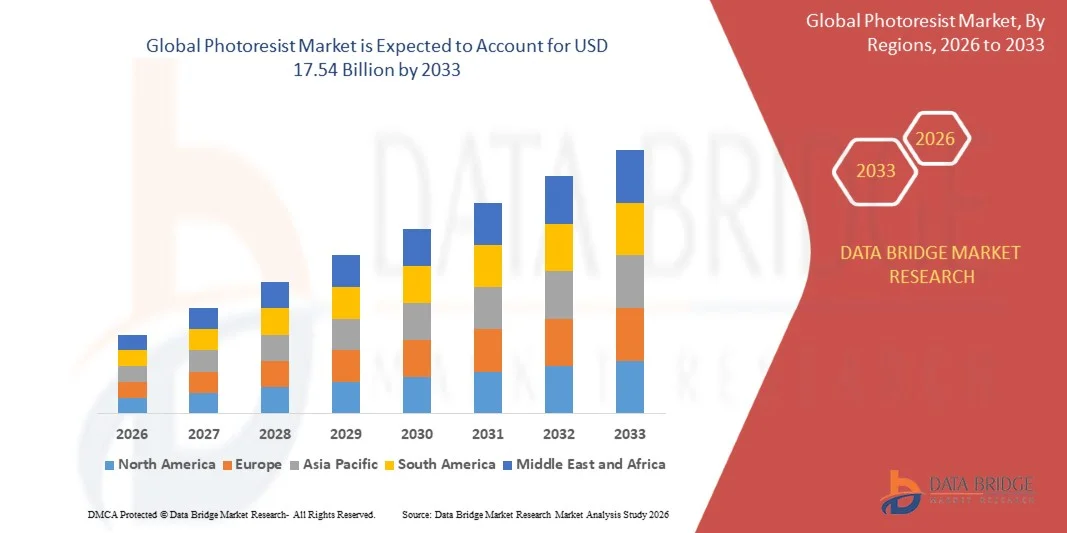
As per Data Bridge Market Research Analysis the photoresist market was valued at USD 11.39 billion in 2025 and is projected to reach USD 17.54 billion by 2033, growing at a CAGR of 5.55% from 2026 to 2033. The market is witnessing steady growth due to the increasing demand for advanced semiconductor devices, rapid technological advancements in photolithography processes, and rising investments in semiconductor fabrication facilities worldwide. The growing adoption of artificial intelligence (AI), 5G communication, Internet of Things (IoT), electric vehicles (EVs), and high-performance computing is accelerating semiconductor production, thereby driving the demand for high-performance photoresist materials used in integrated circuits (ICs), printed circuit boards (PCBs), liquid crystal displays (LCDs), and organic light-emitting diode (OLED) manufacturing.
The market is also benefiting from growing demand for advanced packaging technologies, automotive electronics, data centers, and display manufacturing, all of which require high-purity and high-performance photoresist materials.
Market Size & Forecast
- Global Market Value (2025): USD 11.39 Billion
- Expected Market Value (2033): USD 17.54 Billion
- Forecast CAGR (2026–2033): 5.55%
- Leading Region in 2025: Asia-Pacific
- Fastest Growing Region: North America
Key Market Trends & Insights
- Asia-Pacific dominated the photoresist market with the largest revenue share of 72.85% in 2025, supported by the presence of leading semiconductor fabrication facilities, strong electronics manufacturing capabilities, and substantial investments in advanced wafer production across China, Taiwan, South Korea, and Japan.
- North America is expected to witness the fastest growth during the forecast period, registering a CAGR of 11.49%, driven by increasing investments in domestic semiconductor manufacturing, expansion of advanced fabrication facilities under the CHIPS and Science Act, and growing demand for AI, high-performance computing, and automotive semiconductor applications.
- Positive photoresist dominated the market by type with a 71.91% revenue share in 2025, owing to its superior resolution, high sensitivity, and extensive adoption in advanced semiconductor lithography and integrated circuit manufacturing.
- Extreme ultraviolet (EUV) metal-oxide and dry photoresists are expected to register the fastest growth, expanding at a CAGR of 12.94% during the forecast period, supported by increasing deployment of High-NA EUV lithography for sub-5 nm semiconductor manufacturing.
- Semiconductors and integrated circuits (ICs) accounted for the largest application share of 55.25% in 2025, driven by rising demand for AI accelerators, memory chips, high-performance processors, and advanced logic devices.
- Electricals and electronics remained the largest end-use industry, accounting for 61.75% of the market in 2025, supported by growing production of consumer electronics, data center infrastructure, communication devices, and automotive electronic systems.
Report Scope and Photoresist MarketSegmentation
|
Attributes |
Photoresist Key Market Insights |
|
Segments Covered |
|
|
Countries Covered |
North America
Europe
Asia-Pacific
Middle East and Africa
South America
|
|
Key Market Players |
|
|
Market Opportunities |
|
|
Value Added Data Infosets |
In addition to the insights on market scenarios such as market value, growth rate, segmentation, geographical coverage, and major players, the market reports curated by the Data Bridge Market Research also include import export analysis, production capacity overview, production consumption analysis, price trend analysis, climate change scenario, supply chain analysis, value chain analysis, raw material/consumables overview, vendor selection criteria, PESTLE Analysis, Porter Analysis, and regulatory framework. |
Photoresist Market Trends
Trend: Accelerating Adoption of EUV Lithography and AI-Driven Semiconductor Manufacturing
The photoresist market is witnessing rapid growth as semiconductor manufacturers increasingly adopt extreme ultraviolet (EUV) lithography and prepare for High-NA EUV technology to support advanced semiconductor nodes. Rising demand for artificial intelligence (AI), high-performance computing (HPC), advanced memory, and chiplet-based architectures is increasing the need for high-performance photoresists with superior resolution, sensitivity, and etch resistance. In 2024, JSR Corporation expanded its global development and production capabilities by establishing a new photoresist R&D center in Japan and a manufacturing facility at JSR Micro Korea Co., Ltd. to support the commercialization of Metal Oxide Resist (MOR) for EUV lithography. This investment highlights the growing demand for next-generation photoresist materials. Governments are also supporting domestic semiconductor manufacturing through initiatives such as the CHIPS Act, further accelerating demand for advanced photoresist technologies.
Photoresist Market Dynamics
Key Market Driver: Rising Investments in Advanced Semiconductor Manufacturing
The rapid expansion of the semiconductor industry is the primary driver of the photoresist market. Increasing demand for advanced logic chips, memory devices, artificial intelligence (AI) processors, high-performance computing (HPC), 5G infrastructure, and automotive electronics is encouraging semiconductor manufacturers to expand fabrication capacity worldwide. Governments across the U.S., Europe, Japan, South Korea, and China are also investing heavily in domestic semiconductor manufacturing through various incentive programs, accelerating the adoption of advanced photoresist materials required for high-precision photolithography processes. April 2024, Taiwan Semiconductor Manufacturing Company (TSMC) announced plans to expand its investment in Arizona to more than USD 65 billion, including three advanced semiconductor fabrication plants to support leading-edge chip production. Such investments are expected to significantly increase demand for next-generation EUV and ArF photoresist materials used in advanced semiconductor manufacturing.
Key Restraint/Challenge: Fluctuating Raw Material Prices and Environmental Concerns
One of the major challenges facing the photoresist market is the high production cost and technical complexity associated with advanced photoresist formulations, particularly those designed for Extreme Ultraviolet (EUV) lithography. Manufacturing high-purity photoresists requires sophisticated raw materials, stringent quality control, and specialized production processes, resulting in higher development and manufacturing costs. In addition, the continuous evolution of semiconductor process nodes requires ongoing research and development investments, creating significant barriers for new entrants and increasing operational costs for existing manufacturers. Tokyo Ohka Kogyo Co., Ltd. (TOK) states that it continues to research, develop, and manufacture EUV photoresists approved for mass-production lines, highlighting the significant technological expertise, high-purity manufacturing capabilities, and continuous R&D investment required to support next-generation semiconductor fabrication. These factors, combined with fluctuating raw material prices and increasingly stringent environmental regulations governing chemical manufacturing, continue to challenge profitability and production scalability across the industry.
Key Market Opportunity: Growing Demand for Sustainable and High-Performance Protective Films
The increasing commercialization of extreme ultraviolet (EUV) lithography and the transition toward high-NA EUV semiconductor manufacturing present significant growth opportunities for the photoresist market. As semiconductor manufacturers continue developing sub-5 nm and next-generation chip technologies, demand for high-resolution photoresists with improved sensitivity, pattern fidelity, and etch resistance is expected to increase substantially. Furthermore, rising investments in advanced wafer fabrication facilities, AI semiconductor production, and next-generation memory technologies are expected to create long-term growth opportunities for photoresist manufacturers throughout the forecast period. October 2024, DuPont completed a significant expansion of its photoresist manufacturing capacity at its Sasakami site in Niigata, Japan, by opening the new East Star Building to support the growing global demand for advanced semiconductor photoresists. The expansion strengthens DuPont's ability to supply next-generation photoresist materials for advanced semiconductor manufacturing and reflects the increasing commercialization opportunities created by EUV lithography.
Photoresist Market Scope
The photoresist market is segmented on the basis of type, chemical structure, product type, application, and end-use industry.
- By Type
On the basis of type, the photoresist market is segmented into positive photoresist and negative photoresist. The positive photoresist segment dominated the market with a 71.91% revenue share in 2025, owing to its superior resolution, excellent pattern fidelity, and widespread adoption in advanced semiconductor lithography for integrated circuits (ICs), memory chips, and logic devices. Positive photoresists are extensively used in ArF immersion and EUV lithography processes because they enable the fabrication of fine circuit patterns required for next-generation semiconductor manufacturing.
The negative photoresist segment is expected to witness the fastest growth, registering a CAGR of 11.38% from 2026 to 2033, driven by its increasing use in self-aligned double-patterning, MEMS fabrication, microfluidic devices, and advanced packaging applications. Growing demand for high-aspect-ratio structures, improved mechanical stability, and enhanced process performance in advanced semiconductor manufacturing is expected to accelerate the adoption of negative photoresists during the forecast period.
- By Chemical Structure
On the basis of chemical structure, the photoresist market is segmented into photopolymeric photoresist, photodecomposing photoresist, and photocrosslinking photoresist. The photopolymeric photoresist segment is expected to account for a significant share of the market owing to its excellent photosensitivity, superior adhesion, and high-resolution patterning capabilities, making it widely used in semiconductor fabrication, printed circuit boards (PCBs), and microelectronic manufacturing. Its compatibility with advanced lithography processes and ability to produce precise micro-scale patterns continue to support its widespread adoption across the semiconductor industry.
The photocrosslinking photoresist segment is anticipated to witness strong growth during the forecast period due to its enhanced chemical resistance, mechanical stability, and suitability for high-aspect-ratio microfabrication applications. Increasing demand for advanced packaging, MEMS devices, sensors, and next-generation semiconductor manufacturing technologies is expected to drive the adoption of photocrosslinking photoresists, while photodecomposing photoresists continue to find applications in conventional photolithography processes requiring high pattern accuracy and process reliability.
- By Product Type
On the basis of product type, the photoresist market is segmented into ARF immersion photoresist, ARF dry photoresist, KrF photoresist, G-line photoresist, I-line photoresist, Extreme Ultraviolet (EUV) photoresist, Anti-reflective Coatings, Developers, Removers, and Others. The ARF immersion photoresist segment dominated the market with a 44.00% revenue share in 2025, owing to its superior resolution, enhanced depth of focus, and widespread adoption in advanced semiconductor manufacturing for producing high-density integrated circuits and memory devices. The increasing demand for sub-10 nm process technologies and advanced logic chips continues to support the strong adoption of ARF immersion photoresists across leading semiconductor fabrication facilities. (Grand View Research)
The extreme ultraviolet (EUV) photoresist segment is expected to witness the fastest growth during the forecast period, driven by the rapid commercialization of High-NA EUV lithography, increasing investments in next-generation semiconductor fabrication plants, and rising demand for artificial intelligence (AI), high-performance computing (HPC), and advanced memory chips. Furthermore, growing adoption of anti-reflective coatings, developers, and removers to improve lithography accuracy and manufacturing efficiency is expected to further support the expansion of the product type segment throughout the forecast period.
- By Application
On the basis of application, the photoresist market is segmented into Semiconductors and Integrated Circuits (ICs), Liquid-crystal Displays (LCDs), Organic Light-emitting Diodes (OLEDs), Microelectronics, Printed Circuit Boards, Microcontact Printing, and Others. The Semiconductors and Integrated Circuits (ICs) segment dominated the market with a 55.25% revenue share in 2025, owing to the increasing demand for advanced logic and memory chips, AI accelerators, high-performance computing (HPC), and 5G-enabled devices. The growing adoption of advanced lithography technologies, coupled with rising investments in semiconductor fabrication facilities worldwide, continues to strengthen the demand for high-performance photoresist materials in semiconductor manufacturing.
The Microelectronics segment is expected to witness significant growth during the forecast period, driven by the increasing miniaturization of electronic components, rapid expansion of consumer electronics, and growing demand for wearable devices, IoT products, and advanced sensing technologies. In addition, the rising adoption of advanced packaging technologies, including fan-out wafer-level packaging (FOWLP) and 3D chip integration, is expected to further accelerate the use of photoresists across emerging microelectronic applications.
- End-Use Industry
On the basis of end-use industry, the photoresist market is segmented into electricals and electronics, automobiles, packaging, and others. The electricals and electronics segment dominated the market with a 61.75% revenue share in 2025, owing to the increasing production of semiconductors, integrated circuits, consumer electronics, smartphones, laptops, data center equipment, and communication devices. Rising demand for advanced semiconductor fabrication, coupled with the growing adoption of artificial intelligence (AI), 5G infrastructure, and high-performance computing (HPC), continues to drive the consumption of high-performance photoresist materials across the electronics industry.
The automobiles segment is expected to witness the fastest growth, registering a CAGR of 11.86% from 2026 to 2033, driven by the rapid electrification of vehicles, increasing semiconductor content in electric vehicles (EVs), advanced driver-assistance systems (ADAS), autonomous driving technologies, and automotive power electronics. The growing use of silicon carbide (SiC) power devices, automotive sensors, and advanced packaging technologies is further expected to accelerate the demand for photoresists in automotive semiconductor manufacturing during the forecast period.
Photoresist Market Regional Analysis
Asia-Pacific dominated the photoresist market and accounted for the largest revenue share of 72.85% in 2025, driven by the strong presence of semiconductor manufacturing hubs in Taiwan, South Korea, Japan, and China. The region benefits from high concentrations of leading-edge wafer fabrication facilities, robust consumer electronics production, and continuous investments in advanced lithography technologies. Growing demand for AI processors, memory chips, 5G devices, and high-performance computing (HPC) has further strengthened the consumption of advanced photoresist materials across the region.
Asia-Pacific Photoresist Market Insight
The Asia-Pacific photoresist market continues to lead globally owing to the presence of major semiconductor foundries, display manufacturers, and electronics companies. Countries such as Taiwan, South Korea, Japan, and China account for a significant share of global wafer production and advanced chip manufacturing, resulting in substantial demand for ArF immersion, KrF, and EUV photoresists. Continuous investments in semiconductor fabrication facilities and government support for domestic chip manufacturing are expected to sustain the region's market leadership.
Japan Photoresist Market Insight
The Japan photoresist market remains a key contributor due to the country's leadership in semiconductor materials and specialty chemicals. Japanese manufacturers are among the world's leading suppliers of high-purity photoresists and lithography materials used in advanced semiconductor fabrication. Ongoing investments in research and development, coupled with strong expertise in semiconductor process materials, continue to reinforce Japan's strategic position in the global photoresist industry.
China Photoresist Market Insight
The China photoresist market is expanding rapidly as the country accelerates investments in domestic semiconductor manufacturing and mature-node fabrication capacity. Increasing government support, rising demand for consumer electronics, and efforts to strengthen local supply chains are driving the adoption of photoresist materials. While advanced EUV photoresists remain subject to technology restrictions, continued investments in ArF dry and KrF photoresists, along with expanding 28 nm and mature-node production, are expected to support sustained market growth.
North America Photoresist Market Insight
The North America photoresist market is expected to witness the fastest growth during the forecast period, registering a CAGR of 11.49%, driven by increasing investments in domestic semiconductor manufacturing and the rapid expansion of advanced wafer fabrication facilities across the United States. Government initiatives such as the CHIPS and Science Act are encouraging leading semiconductor manufacturers to establish new fabrication plants in Arizona, Ohio, and Texas, thereby increasing demand for advanced photoresists and ancillary materials. The growing adoption of Extreme Ultraviolet (EUV) lithography, rising production of AI accelerators, high-performance computing (HPC) chips, automotive semiconductors, and advanced packaging technologies are further strengthening the regional market. In addition, photoresist suppliers are expanding local production and blending facilities to improve supply chain resilience and support the growing semiconductor ecosystem, positioning North America as the fastest-growing regional market for photoresists.
U.S. Photoresist Market Insight
The U.S. photoresist market is witnessing strong growth due to increasing investments in domestic semiconductor manufacturing supported by the CHIPS and Science Act. The expansion of fabrication facilities by leading semiconductor manufacturers, coupled with rising demand for AI, defense electronics, and advanced computing applications, is driving the adoption of high-performance photoresists. In addition, investments in EUV lithography and advanced packaging technologies are strengthening the country's position in the semiconductor materials market.
Germany Photoresist Market Insight
The Germany photoresist market is experiencing steady growth, supported by expanding semiconductor manufacturing capabilities and increasing investments in advanced microelectronics. Government-backed initiatives and large-scale investments in new fabrication facilities are encouraging the adoption of advanced lithography materials. The country's strong industrial base and focus on automotive semiconductors, industrial automation, and high-performance electronics continue to support market expansion.
Photoresist Market Share
The photoresist industry is primarily led by well-established companies, including:
- JSR Corporation (Japan)
- Tokyo Ohka Kogyo Co., Ltd. (Japan)
- Shin-Etsu Chemical Co., Ltd. (Japan)
- Fujifilm Holdings Corporation (Japan)
- Merck KGaA, Darmstadt (Germany)
- DuPont (U.S.)
- Sumitomo Chemical Co., Ltd. (Japan)
- Dongjin Semichem Co., Ltd. (South Korea)
- Allresist DE (Germany)
- MicroCHEM (U.S.)
- Kayaku AM (U.S.)
- LG Chem (South Korea)
- SAMSUNG SDI. (South Korea)
- Mitsubishi Chemical Corporation. (Japan)
- Resonac Holdings Corporation (Japan)
- BASF (Germany)
- Entegris (U.S.)
- Brewer Science, Inc. (U.S.)
- Eternal Materials Co., Ltd. (Taiwan)
- KUMHO PETROCHEMICAL. (South Korea)
Latest Developments in Photoresist Market
- In June 2025, JSR Corporation announced plans to strengthen its next-generation semiconductor materials portfolio by accelerating the development of Extreme Ultraviolet (EUV) photoresists and advanced lithography materials to support sub-2 nm semiconductor manufacturing. The initiative is expected to enhance patterning performance and meet the growing demand for AI, high-performance computing (HPC), and advanced memory applications.
- In February 2025, Resonac Holdings Corporation announced the establishment of a new research and development center in Silicon Valley, U.S., dedicated to next-generation semiconductor packaging materials. The facility is intended to strengthen collaboration with U.S. semiconductor companies and accelerate the development of advanced semiconductor materials.
- In 2025, Fujifilm Electronic Materials continued expanding its semiconductor materials business by enhancing its portfolio of photoresists and process chemicals for advanced logic and memory devices. The company is investing in next-generation lithography materials to support advanced chip manufacturing and strengthen semiconductor supply chains.
- Interactive Data Analysis Dashboard
- Company Analysis Dashboard for high growth potential opportunities
- Research Analyst Access for customization & queries
- Competitor Analysis with Interactive dashboard
- Latest News, Updates & Trend analysis
- Harness the Power of Benchmark Analysis for Comprehensive Competitor Tracking
Global Photoresist Market, Supply Chain Analysis and Ecosystem Framework
To support market growth and help clients navigate the impact of geopolitical shifts, DBMR has integrated in-depth supply chain analysis into its Global Photoresist Market research reports. This addition empowers clients to respond effectively to global changes affecting their industries. The supply chain analysis section includes detailed insights such as Global Photoresist Market consumption and production by country, price trend analysis, the impact of tariffs and geopolitical developments, and import and export trends by country and HSN code. It also highlights major suppliers with data on production capacity and company profiles, as well as key importers and exporters. In addition to research, DBMR offers specialized supply chain consulting services backed by over a decade of experience, providing solutions like supplier discovery, supplier risk assessment, price trend analysis, impact evaluation of inflation and trade route changes, and comprehensive market trend analysis.
Data collection and base year analysis are done using data collection modules with large sample sizes. The stage includes obtaining market information or related data through various sources and strategies. It includes examining and planning all the data acquired from the past in advance. It likewise envelops the examination of information inconsistencies seen across different information sources. The market data is analysed and estimated using market statistical and coherent models. Also, market share analysis and key trend analysis are the major success factors in the market report. To know more, please request an analyst call or drop down your inquiry.
The key research methodology used by DBMR research team is data triangulation which involves data mining, analysis of the impact of data variables on the market and primary (industry expert) validation. Data models include Vendor Positioning Grid, Market Time Line Analysis, Market Overview and Guide, Company Positioning Grid, Patent Analysis, Pricing Analysis, Company Market Share Analysis, Standards of Measurement, Global versus Regional and Vendor Share Analysis. To know more about the research methodology, drop in an inquiry to speak to our industry experts.
Data Bridge Market Research is a leader in advanced formative research. We take pride in servicing our existing and new customers with data and analysis that match and suits their goal. The report can be customized to include price trend analysis of target brands understanding the market for additional countries (ask for the list of countries), clinical trial results data, literature review, refurbished market and product base analysis. Market analysis of target competitors can be analyzed from technology-based analysis to market portfolio strategies. We can add as many competitors that you require data about in the format and data style you are looking for. Our team of analysts can also provide you data in crude raw excel files pivot tables (Fact book) or can assist you in creating presentations from the data sets available in the report.