

What is the Semiconductor Bonding Market Size and Growth Rate?
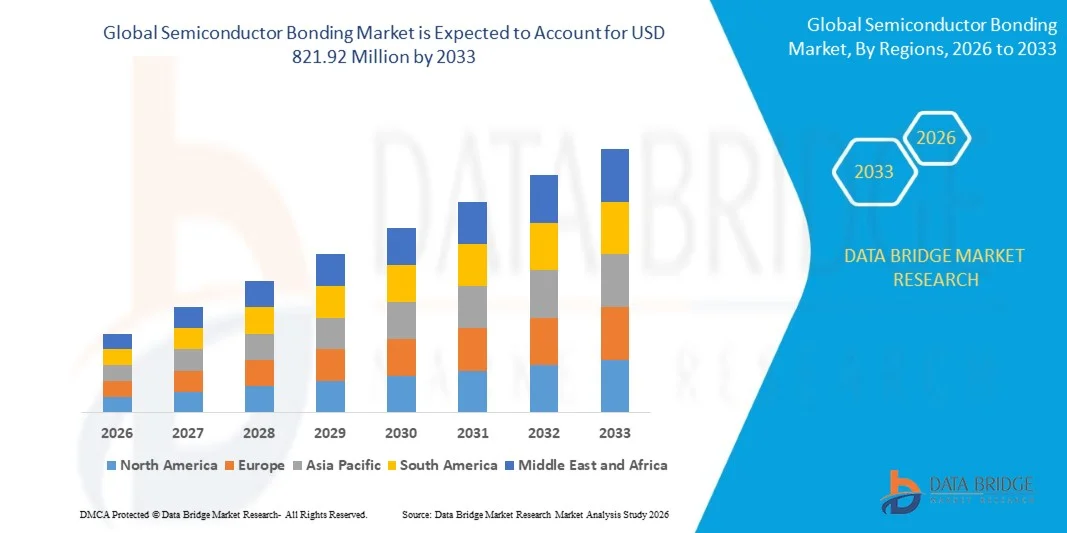
- As per Data Bridge Market Research analysis the semiconductor bonding market was valued at USD 569.19 million in 2025 and is projected to reach USD 821.92 million by 2033, growing at a CAGR of 4.70% from 2026 to 2033.
- The market is experiencing consistent growth driven by increasing demand for advanced semiconductor packaging, rising adoption of 3D and heterogeneous integration technologies, and growing applications across consumer electronics, automotive, telecommunications, and high-performance computing.
- The increasing complexity of semiconductor devices, combined with the need for higher interconnect density, improved thermal performance, and miniaturized components, is compelling semiconductor manufacturers and packaging companies to adopt advanced bonding technologies.
Market Size & Forecast
- Market Value (2025): USD 569.19 Million
- Expected Market Value (2033): USD 821.92 Million
- Forecast CAGR (2026–2033): 4.70%
- Leading Region in 2025: North America
- Fastest Growing Region: Asia-Pacific
What are the Major Takeaways of the Semiconductor Bonding Market?
- North America dominated the semiconductor bonding market with the largest revenue share of 36.90% in 2025, supported by strong semiconductor manufacturing capabilities, increasing investment in advanced packaging, and growing demand for high-performance computing technologies.
- Asia-Pacific semiconductor bonding market is expected to witness the fastest growth rate from 2026 to 2034, supported by rapid semiconductor manufacturing expansion, increasing investments in advanced packaging, and growing demand for consumer electronics and high-performance computing.
- The die-to-die bonding segment held the largest market revenue share of approximately 52.39% in 2025, driven by its superior electrical and thermal performance in high-performance computing and advanced semiconductor applications. Die-to-die bonding is preferred due to its precise alignment, flexibility, and ability to support high-density semiconductor integration.
- The die-to-wafer bonding segment is projected to register the fastest growth at a CAGR higher than the overall market CAGR from 2026 to 2033, driven by its scalability and cost efficiency for mass production. Increasing adoption in advanced packaging and heterogeneous integration applications is accelerating segment expansion.
- The die bonding segment held a significant position in the market in 2025, supported by its widespread use in semiconductor assembly and packaging applications. Die bonding is preferred due to its reliable chip attachment, precise placement, and suitability for diverse semiconductor manufacturing requirements.
- The hybrid bonding segment is projected to register the fastest growth at a CAGR higher than the overall market CAGR from 2026 to 2033, driven by increasing adoption in next-generation semiconductor integration and advanced 3D packaging. Rising demand for higher interconnect density and improved device performance is accelerating segment expansion.
Report Scope and Semiconductor Bonding Market Segmentation
|
Attributes |
Semiconductor Bonding Key Market Insights |
|
Segments Covered |
|
|
Countries Covered |
North America
Europe
Asia-Pacific
Middle East and Africa
South America
|
|
Key Market Players |
|
|
Market Opportunities |
|
|
Value Added Data Infosets |
In addition to the insights on market scenarios such as market value, growth rate, segmentation, geographical coverage, and major players, the market reports curated by the Data Bridge Market Research also include in-depth expert analysis, geographically represented company-wise production and capacity, network layouts of distributors and partners, detailed and updated price trend analysis and deficit analysis of supply chain and demand. |
What is the Key Trend in the Semiconductor Bonding Market?
- Semiconductor manufacturers are increasingly adopting hybrid bonding and die-to-wafer bonding technologies to enable higher interconnect density, smaller chip packages, and improved performance for advanced logic, memory, and AI applications.
- For instance, in October 2025, Applied Materials introduced the Kinex bonding system, an integrated die-to-wafer hybrid bonding system designed to support higher-performance and lower-power advanced logic and memory chips.
- Hybrid bonding enables direct copper-to-copper connections, supporting smaller interconnect pitches while improving performance, power efficiency, and integration in complex multi-chip packages.
- Semiconductor equipment manufacturers are also increasing their focus on high-precision metrology to improve alignment accuracy and bonding yields as chiplet and 3D integration requirements become more demanding.
- For instance, in September 2025, EV Group introduced the EVG40 D2W overlay metrology system, which provides 100% die overlay measurement on 300-mm wafers and measures up to 2,800 overlay points in four minutes.
- As AI, high-performance computing, high-bandwidth memory, and chiplet architectures continue expanding, adoption of hybrid bonding and precision bonding technologies is expected to accelerate.
What are the Key Drivers of the Semiconductor Bonding Market?
- The rapid expansion of artificial intelligence, high-performance computing, advanced memory, and chiplet-based architectures is significantly increasing demand for advanced semiconductor packaging and bonding technologies.
- For instance, in October 2025, Applied Materials stated that its Kinex system was developed to support advanced logic and memory chips used in AI computing by enabling high-accuracy die-to-wafer hybrid bonding and smaller interconnect pitches.
- Semiconductor manufacturers are increasingly using die-to-wafer and wafer-to-wafer bonding to integrate multiple chips and chiplets while improving interconnect density, power efficiency, and overall system performance.
- For instance, in September 2025, EV Group highlighted its wafer-to-wafer and die-to-wafer hybrid bonding solutions for chiplet integration, high-bandwidth memory stacks, and advanced 3D packaging applications.
- The increasing complexity of semiconductor architectures, combined with the need for smaller form factors and higher processing performance, is encouraging manufacturers to invest in advanced bonding equipment and packaging technologies.
• As semiconductor scaling increasingly depends on heterogeneous integration and advanced packaging, demand for die bonding, hybrid bonding, thermocompression bonding, and related equipment is expected to remain strong.
Which Factors are Challenging the Growth of the Semiconductor Bonding Market?
- Advanced semiconductor bonding requires extremely precise alignment, surface preparation, cleanliness, and process control, increasing equipment complexity and manufacturing costs.
- These requirements can create challenges in achieving high bonding yields, particularly for high-volume production of fine-pitch and three-dimensional semiconductor devices.
- For instance, in September 2025, EV Group highlighted that tighter interconnect pitches in 3D packaging require greater die-bond alignment accuracy and comprehensive metrology to identify overlay errors that can cause misaligned copper pads, bond interfaces, and yield losses.
- Semiconductor manufacturers must also invest in advanced metrology, inspection, wafer preparation, and bonding equipment to maintain process consistency as interconnect dimensions continue to shrink.
- The high capital investment, stringent process requirements, and technical complexity associated with advanced bonding can limit adoption among smaller manufacturers and increase semiconductor packaging costs.
- These cost and manufacturing challenges may slow adoption of advanced bonding technologies in price-sensitive applications despite growing demand for high-performance and highly integrated semiconductor devices.
How is the Semiconductor Bonding Market Segmented?
The market is segmented on the basis of process type, technology, application, and type.
- By Process Type
On the basis of process type, the semiconductor bonding market is segmented into die-to-die bonding, die-to-wafer bonding, and wafer-to-wafer bonding. The die-to-die bonding segment held the largest market revenue share of approximately 52.39% in 2025, driven by its superior electrical and thermal performance in high-performance computing and advanced semiconductor applications. Die-to-die bonding is preferred due to its precise alignment, flexibility, and ability to support high-density semiconductor integration.
The die-to-wafer bonding segment is projected to register the fastest growth at a CAGR higher than the overall market CAGR from 2026 to 2033, driven by its scalability and cost efficiency for mass production. Increasing adoption in advanced packaging and heterogeneous integration applications is accelerating segment expansion.
- By Technology
On the basis of technology, the semiconductor bonding market is segmented into die bonding, epoxy die bonding, eutectic die bonding, flip-chip attachment, and hybrid bonding. The die bonding segment held a significant position in the market in 2025, supported by its widespread use in semiconductor assembly and packaging applications. Die bonding is preferred due to its reliable chip attachment, precise placement, and suitability for diverse semiconductor manufacturing requirements.
The hybrid bonding segment is projected to register the fastest growth at a CAGR higher than the overall market CAGR from 2026 to 2033, driven by increasing adoption in next-generation semiconductor integration and advanced 3D packaging. Rising demand for higher interconnect density and improved device performance is accelerating segment expansion.
- By Application
On the basis of application, the semiconductor bonding market is segmented into advanced packaging, Micro-Electro-Mechanical Systems (MEMS) fabrication, RF devices, LEDs and photonics, CMOS image sensor (CIS) manufacturing, and others. The MEMS fabrication segment held the largest market revenue share of approximately 26.66% in 2025, driven by widespread use of MEMS components in smartphones, automotive sensors, medical equipment, and industrial systems. MEMS fabrication is preferred due to the growing demand for compact, precise, and highly integrated sensing technologies.
The advanced packaging segment is projected to register the fastest growth at a CAGR higher than the overall market CAGR from 2026 to 2033, driven by increasing adoption of 3D stacking and wafer-level packaging technologies. Rising demand for high-performance computing, artificial intelligence, and miniaturized semiconductor devices is accelerating segment expansion.
- By Type
On the basis of type, the semiconductor bonding market is segmented into flip-chip bonders, wafer bonders, wire bonders, hybrid bonders, die bonders, thermocompression bonders, and others. The die bonders segment held the largest market revenue share of approximately 32.37% in 2025, driven by its essential role in semiconductor assembly across consumer electronics, automotive, and telecommunications applications. Die bonders are preferred due to their precise chip placement, reliable attachment, and compatibility with high-volume semiconductor manufacturing.
The hybrid bonders segment is projected to register the fastest growth at a CAGR higher than the overall market CAGR from 2026 to 2033, driven by their increasing role in next-generation semiconductor integration. Growing demand for advanced packaging, high-density interconnects, and 3D semiconductor architectures is accelerating segment expansion.
Which Region Holds the Largest Share of the Semiconductor Bonding Market?
- North America dominated the semiconductor bonding market with the largest revenue share of 36.90% in 2025, supported by strong semiconductor manufacturing capabilities, increasing investment in advanced packaging, and growing demand for high-performance computing technologies.
- The region benefits from the presence of major semiconductor manufacturers, equipment suppliers, and research institutions focused on chiplet integration, 3D packaging, and advanced bonding technologies. Rising investments in artificial intelligence, data centers, and next-generation semiconductor infrastructure are further supporting the adoption of advanced bonding solutions.
U.S. Semiconductor Bonding Market Insight
U.S. semiconductor bonding market captured the largest revenue share in North America in 2025, fueled by increasing investments in semiconductor manufacturing, advanced packaging, and artificial intelligence infrastructure. The country's strong ecosystem of semiconductor manufacturers and equipment providers is accelerating the adoption of die-to-wafer, hybrid bonding, and thermocompression bonding technologies. Moreover, government initiatives supporting domestic semiconductor production and increasing demand for high-performance chips are contributing significantly to market expansion.
Europe Semiconductor Bonding Market Insight
Europe semiconductor bonding market is expected to witness steady growth from 2026 to 2034, primarily driven by increasing investments in semiconductor manufacturing, automotive electronics, and advanced packaging technologies. The region's emphasis on semiconductor supply-chain resilience and technological sovereignty is encouraging the development of localized manufacturing capabilities. Growing demand for MEMS, sensors, power electronics, and heterogeneous integration is further supporting the adoption of advanced semiconductor bonding technologies.
U.K. Semiconductor Bonding Market Insight
U.K. semiconductor bonding market is expected to witness strong growth from 2026 to 2034, driven by increasing investments in semiconductor research, advanced packaging, and high-performance electronic systems. The country's established research ecosystem and focus on semiconductor innovation are supporting the development of advanced bonding and packaging technologies. Moreover, growing demand for semiconductor components across automotive, telecommunications, aerospace, and defense applications is expected to stimulate market growth.
Germany Semiconductor Bonding Market Insight
Germany semiconductor bonding market is expected to witness significant growth from 2026 to 2034, fueled by its strong automotive semiconductor industry, advanced manufacturing capabilities, and increasing investments in semiconductor production. The country's focus on industrial automation, electric vehicles, power electronics, and sensor technologies is creating demand for reliable semiconductor packaging and bonding solutions. Furthermore, increasing efforts to strengthen domestic semiconductor manufacturing and supply-chain resilience are supporting market expansion.
Asia-Pacific Semiconductor Bonding Market Insight
Asia-Pacific semiconductor bonding market is expected to witness the fastest growth rate from 2026 to 2034, supported by rapid semiconductor manufacturing expansion, increasing investments in advanced packaging, and growing demand for consumer electronics and high-performance computing. Countries such as China, Taiwan, South Korea, and Japan have established semiconductor ecosystems that are accelerating the adoption of wafer bonding, die bonding, and hybrid bonding technologies. Furthermore, increasing investments in artificial intelligence, advanced memory, chiplets, and 3D integration are creating significant opportunities for semiconductor bonding manufacturers.
Japan Semiconductor Bonding Market Insight
Japan semiconductor bonding market is expected to witness strong growth from 2026 to 2034 due to the country's advanced semiconductor manufacturing ecosystem, strong presence in semiconductor materials and equipment, and growing demand for advanced packaging technologies. Increasing applications of bonding technologies in MEMS, image sensors, power devices, and automotive electronics are supporting market growth. Moreover, rising investments in domestic semiconductor production and next-generation packaging technologies are expected to further strengthen demand for semiconductor bonding solutions.
China Semiconductor Bonding Market Insight
China semiconductor bonding market accounted for a significant market revenue share in Asia Pacific in 2025, attributed to rapid expansion of domestic semiconductor manufacturing, increasing investments in advanced packaging, and growing demand for electronic devices. The country's emphasis on strengthening semiconductor self-sufficiency is encouraging investments in wafer bonding, die bonding, and other advanced packaging technologies. Furthermore, increasing production of consumer electronics, electric vehicles, artificial intelligence hardware, and semiconductor components is expected to further propel the semiconductor bonding market in China.
Which are the Top Companies in Semiconductor Bonding Market?
The semiconductor bonding industry is primarily led by well-established companies, including:
- BE Semiconductor Industries N.V. (Netherlands)
- Intel Corporation (U.S.)
- Palomar Technologies, Inc. (U.S.)
- Panasonic Connect Co., Ltd. (Japan)
- Kulicke and Soffa Industries, Inc. (Singapore)
- SHIBAURA MECHATRONICS CORPORATION (Japan)
- TDK Corporation (Japan)
- ASMPT (Singapore)
- Tokyo Electron Limited (Japan)
- EV Group (EVG) (Austria)
- Fasford Technology Co., Ltd. (Japan)
- SUSS MicroTec SE (Germany)
- Mycronic AB (Sweden)
- Shinkawa Ltd. (Japan)
- Applied Materials, Inc. (U.S.)
What are Latest Developments in Semiconductor Bonding Market?
- In July 2024, Hanmi Semiconductor announced a new product development plan to introduce 2.5D big-die thermal compression (TC) bonders in the second half of 2024, targeting the growing AI semiconductor and advanced packaging market. The company planned to expand its TC bonder portfolio beyond HBM applications into 2.5D packaging for large-die and multi-chip integration. The new equipment is expected to support higher-performance semiconductor packaging while expanding Hanmi Semiconductor’s customer base across advanced packaging applications. The development is expected to intensify competition among bonding-equipment manufacturers as demand for AI and HBM packaging continues to increase.
- In June 2024, EV Group (EVG) and Fraunhofer IZM-ASSID expanded their strategic partnership to develop and optimize wafer bonding and debonding technologies for advanced CMOS, heterogeneous integration, and quantum computing applications. Fraunhofer installed EVG’s EVG850 DB fully automated UV laser debonding and cleaning system at the newly established CEASAX center in Dresden. The installation enables in-house processing of thin wafers and supports 300-mm wafer-level 3D integration research. The collaboration is expected to accelerate technology development and strengthen advanced wafer bonding capabilities for quantum and next-generation semiconductor applications.
- In May 2024, ITEC Equipment introduced the ADAT3 XF TwinRevolve flip-chip die bonder, a new high-speed bonding system capable of attaching up to 60,000 flip-chip dies per hour. The system operates five times faster than comparable market-leading bonders and achieves placement accuracy better than 5 μm at 1σ. Its two rotating heads reduce inertia and vibration while enabling faster and smoother die placement. The technology is expected to lower factory space and operating costs while supporting broader adoption of flip-chip packaging in high-performance semiconductor applications.
- In August 2023, EV Group showcased its latest hybrid bonding, metrology, and nanoimprint lithography technologies at SEMICON Taiwan 2023, focusing on wafer-to-wafer and die-to-wafer bonding for 3D and heterogeneous integration. The company highlighted applications in next-generation logic and memory manufacturing, chiplet integration, and advanced semiconductor packaging. These technologies are designed to enable higher interconnect density, improved integration, and reliable production yields. The development is expected to support the industry’s transition toward advanced 3D semiconductor architectures and strengthen demand for high-precision bonding equipment.
- In August 2023, Kulicke and Soffa Industries announced a collaboration with Taiwan Surface Mounting Technology Corp. (TSMT) to advance its LUMINEX laser-based mini and micro LED die transfer technology. The collaboration focuses on developing mini LED backlight and direct-emissive display applications for high-volume adoption by combining laser technology, optical systems, material engineering, and precision motion control. The solution is designed to provide high throughput and placement accuracy for advanced display manufacturing. The collaboration is expected to expand high-volume die-transfer applications and create additional opportunities for advanced semiconductor and display packaging technologies.
- Interactive Data Analysis Dashboard
- Company Analysis Dashboard for high growth potential opportunities
- Research Analyst Access for customization & queries
- Competitor Analysis with Interactive dashboard
- Latest News, Updates & Trend analysis
- Harness the Power of Benchmark Analysis for Comprehensive Competitor Tracking
Global Semiconductor Bonding Market, Supply Chain Analysis and Ecosystem Framework
To support market growth and help clients navigate the impact of geopolitical shifts, DBMR has integrated in-depth supply chain analysis into its Global Semiconductor Bonding Market research reports. This addition empowers clients to respond effectively to global changes affecting their industries. The supply chain analysis section includes detailed insights such as Global Semiconductor Bonding Market consumption and production by country, price trend analysis, the impact of tariffs and geopolitical developments, and import and export trends by country and HSN code. It also highlights major suppliers with data on production capacity and company profiles, as well as key importers and exporters. In addition to research, DBMR offers specialized supply chain consulting services backed by over a decade of experience, providing solutions like supplier discovery, supplier risk assessment, price trend analysis, impact evaluation of inflation and trade route changes, and comprehensive market trend analysis.
Data collection and base year analysis are done using data collection modules with large sample sizes. The stage includes obtaining market information or related data through various sources and strategies. It includes examining and planning all the data acquired from the past in advance. It likewise envelops the examination of information inconsistencies seen across different information sources. The market data is analysed and estimated using market statistical and coherent models. Also, market share analysis and key trend analysis are the major success factors in the market report. To know more, please request an analyst call or drop down your inquiry.
The key research methodology used by DBMR research team is data triangulation which involves data mining, analysis of the impact of data variables on the market and primary (industry expert) validation. Data models include Vendor Positioning Grid, Market Time Line Analysis, Market Overview and Guide, Company Positioning Grid, Patent Analysis, Pricing Analysis, Company Market Share Analysis, Standards of Measurement, Global versus Regional and Vendor Share Analysis. To know more about the research methodology, drop in an inquiry to speak to our industry experts.
Data Bridge Market Research is a leader in advanced formative research. We take pride in servicing our existing and new customers with data and analysis that match and suits their goal. The report can be customized to include price trend analysis of target brands understanding the market for additional countries (ask for the list of countries), clinical trial results data, literature review, refurbished market and product base analysis. Market analysis of target competitors can be analyzed from technology-based analysis to market portfolio strategies. We can add as many competitors that you require data about in the format and data style you are looking for. Our team of analysts can also provide you data in crude raw excel files pivot tables (Fact book) or can assist you in creating presentations from the data sets available in the report.