
Global Semiconductor Packaging Equipment Market
Market Size in USD Billion
 USD
8.60 Billion
USD
19.20 Billion
2025
2033
USD
8.60 Billion
USD
19.20 Billion
2025
2033
| 2026 - 2033 | |
| USD 8.60 Billion | |
| USD 19.20 Billion | |
| % | |
|
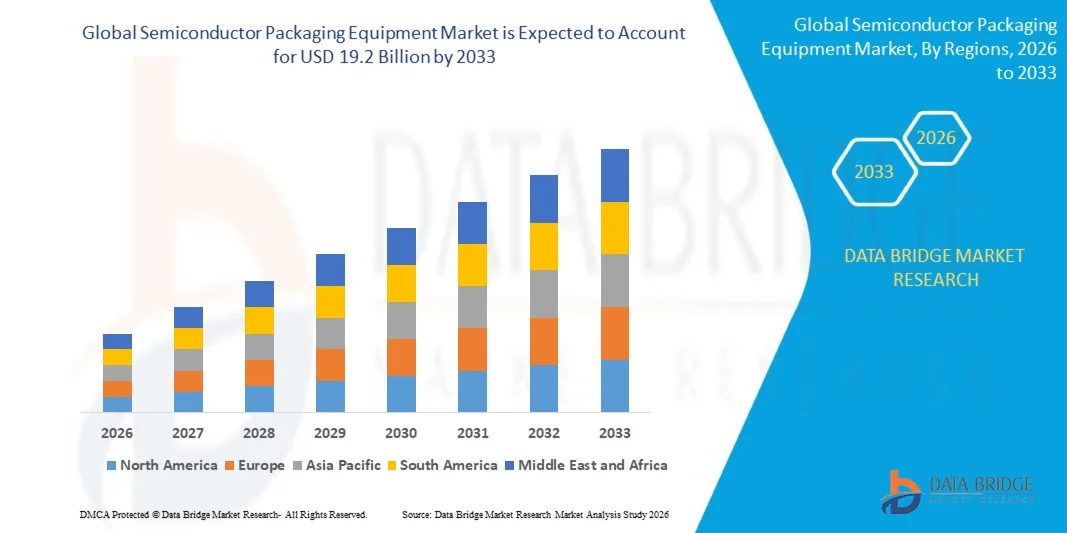
Semiconductor Packaging Equipment Market Size
- The global Semiconductor Packaging Equipment market size was valued at USD 8.6 billion in 2025 and is projected to reach USD 19.2 billion by 2033, registering a CAGR of 10.6% during the forecast period 2026–2033.
- Market growth is primarily driven by the accelerating global demand for advanced semiconductor packaging formats — including 3D/2.5D IC integration, fan-out wafer-level packaging (FOWLP), and chiplet-based heterogeneous integration — fueled by the proliferation of artificial intelligence (AI) accelerators, high-performance computing (HPC) chips, and next-generation 5G devices that require higher interconnect density and bandwidth than conventional packaging solutions can deliver.
- Additionally, rapidly expanding outsourced semiconductor assembly and test (OSAT) capacity in Asia, unprecedented government-backed semiconductor manufacturing investments under the U.S. CHIPS and Science Act and EU Chips Act, growing electrification of the automotive industry driving power semiconductor packaging demand, and rising adoption of advanced wafer-level and flip-chip packaging in consumer electronics and data center applications are collectively sustaining robust market expansion through 2033.
Semiconductor Packaging Equipment Market Analysis
- Semiconductor packaging equipment, utilized across die bonding, wire bonding, flip-chip assembly, wafer-level packaging, encapsulation, molding, electroplating, dicing, and inspection operations, enables the final assembly, interconnection, protection, and quality validation of semiconductor devices — transforming fabricated wafers into functional, deployable electronic components ready for integration into end-product applications.
- The growing demand for semiconductor packaging equipment is driven by the rapid evolution of packaging technology from traditional wire-bonded packages toward advanced multi-die integration formats including 2.5D interposer-based packages, 3D stacked die configurations, and system-in-package (SiP) modules, all of which require increasingly sophisticated precision bonding, alignment, and inspection equipment with capabilities that conventional assembly tools cannot provide.
- Asia-Pacific dominated the Semiconductor Packaging Equipment market with the largest revenue share of approximately 68.0% in 2025, underpinned by the world’s highest concentration of OSAT providers — including ASE Group, Amkor Technology, JCET, and Powertech Technology — as well as leading semiconductor foundries and IDMs in Taiwan, South Korea, China, and Japan that represent the core global demand hub for packaging equipment procurement and advanced packaging technology adoption.
- North America is expected to be the fastest-growing region with a CAGR of approximately 12.8% during the forecast period, driven by historic CHIPS Act-funded semiconductor manufacturing investments generating new domestic advanced packaging capacity, the U.S. CHIPS National Advanced Packaging Manufacturing Program (NAPMP) directing USD 1.4 billion specifically toward domestic packaging infrastructure, strong demand from U.S.-based fabless AI chip leaders including NVIDIA, AMD, and Qualcomm for advanced heterogeneous integration packaging services, and expanding domestic OSAT capacity from Amkor Technology’s Arizona campus.
- The Wire Bonding Equipment segment dominated the market with a share of approximately 30.0% in 2025, reflecting the technology’s continued dominance in high-volume, cost-effective semiconductor assembly across consumer electronics, automotive, and industrial applications where mature wire bonding processes deliver reliable performance at lower cost than flip-chip alternatives.
Report Scope and Semiconductor Packaging Equipment Market Segmentation
|
Attributes |
Semiconductor Packaging Equipment Key Market Insights |
|
Segments Covered |
· By Equipment Type: Die Bonding Equipment, Wire Bonding Equipment, Packaging Equipment, Flip Chip Bonding Equipment, Wafer-Level Packaging Equipment, Inspection & Cutting Equipment, Others · By Packaging Technology: Traditional Packaging, Advanced Packaging (3D/2.5D IC, Fan-Out Wafer-Level Packaging (FOWLP), Wafer-Level Chip-Scale Packaging (WLCSP), System-in-Package (SiP)) · By Application: Integrated Device Manufacturers (IDMs), Outsourced Semiconductor Assembly and Test (OSAT), Foundries · By End-User Industry: Consumer Electronics, Automotive, Telecommunications & 5G, Industrial, Data Centers & AI/HPC, Aerospace & Defense, Others |
|
Countries Covered |
North America: · U.S. · Canada · Mexico Europe: · Germany · France · U.K. · Netherlands · Switzerland · Belgium · Russia · Italy · Spain · Turkey · Rest of Europe Asia-Pacific: · China · Japan · South Korea · Taiwan · India · Singapore · Malaysia · Rest of Asia-Pacific Middle East and Africa: · Saudi Arabia · U.A.E. · South Africa · Egypt · Israel · Rest of MEA South America: · Brazil · Argentina · Rest of South America |
|
Key Market Players |
· ASMPT Limited (Hong Kong) · Kulicke and Soffa Industries Inc. (U.S.) · BE Semiconductor Industries N.V. (Besi) (Netherlands) · TOWA Corporation (Japan) · Tokyo Electron Limited (Japan) · Disco Corporation (Japan) · ASM International N.V. (Netherlands) · SHINKAWA Electric Co. Ltd. (Japan) · SUSS MicroTec SE (Germany) · Advantest Corporation (Japan) · Amkor Technology (U.S.) · NAURA Technology Group Co. Ltd. (China) |
|
Market Opportunities |
• The U.S. CHIPS National Advanced Packaging Manufacturing Program (NAPMP) committing USD 1.4 billion specifically for domestic packaging infrastructure is catalyzing rapid capacity expansion and advanced packaging equipment procurement across North America. • Explosive growth in AI accelerator chip demand from NVIDIA, AMD, Google, and Microsoft is driving unprecedented adoption of 2.5D/3D advanced packaging formats for CoWoS, HBM memory stacking, and chiplet integration, creating premium-value equipment demand. • Rapid electrification of the global automotive industry is creating high-growth demand for power semiconductor packaging equipment capable of handling wide-bandgap SiC and GaN devices for EV inverters, onboard chargers, and advanced driver-assistance systems. |
|
Value Added Data Infosets |
In addition to the insights on market scenarios such as market value, growth rate, segmentation, geographical coverage, and major players, the market reports curated by the Data Bridge Market Research also include in-depth expert analysis, geographically represented company-wise production and capacity, network layouts of distributors and partners, detailed and updated price trend analysis and deficit analysis of supply chain and demand. |
Semiconductor Packaging Equipment Market Trends
“AI Chiplets, EV Growth, and Semiconductor Sovereignty Programs Driving Advanced Packaging Equipment Opportunities”
- Explosive growth in AI accelerator and HPC chip production is driving unprecedented adoption of 2.5D and 3D advanced packaging formats — including NVIDIA’s CoWoS (Chip-on-Wafer-on-Substrate) and AMD’s 3D V-Cache architectures — that require highly specialized precision bonding, hybrid bonding, and advanced inspection equipment operating at sub-micron alignment tolerances far beyond conventional packaging system capabilities.
- Rising adoption of chiplet-based heterogeneous integration as a mainstream chip design strategy — enabling semiconductor companies to combine best-in-class dies from multiple process nodes into a single high-performance package — is creating sustained, premium-value demand for advanced die-to-die bonding equipment, precision interposer assembly tools, and multi-die inspection and metrology systems across leading semiconductor manufacturers globally.
- Rapid global expansion of 5G network infrastructure and the emerging buildout of 6G research programs is driving sustained demand for advanced RF semiconductor packaging equipment capable of handling compound semiconductor devices — particularly gallium nitride (GaN) and indium phosphide (InP) power amplifiers — with tight thermal management and high-frequency electrical performance requirements.
- Accelerating electrification of the global automotive industry is creating a high-growth new market for power semiconductor packaging equipment optimized for wide-bandgap silicon carbide (SiC) and gallium nitride (GaN) devices, with automotive-grade packaging requirements for extended temperature cycling, vibration resistance, and long-term reliability driving specialized equipment development at leading packaging tool manufacturers.
- Growing industry-wide adoption of fan-out wafer-level packaging (FOWLP) and embedded die packaging formats for smartphone application processors, mobile power management ICs, and IoT connectivity chips is expanding demand for advanced molding, redistribution layer (RDL) deposition, and wafer-level testing equipment across both IDM and OSAT production environments.
- Integration of artificial intelligence and machine learning into packaging equipment control systems is enabling real-time defect detection, adaptive process optimization, and predictive maintenance capabilities that reduce yield loss, minimize unplanned downtime, and lower total cost of ownership — creating a competitive differentiation axis for equipment manufacturers investing in smart packaging automation platforms.
- Growing demand for System-in-Package (SiP) solutions in wearable electronics, hearables, true wireless stereo (TWS) earbuds, and implantable medical devices is driving adoption of highly compact, multi-component assembly equipment capable of precisely placing and bonding heterogeneous components including passive elements, sensors, and RF modules within extremely tight package footprint constraints.
- Overall, the semiconductor packaging equipment market is undergoing a fundamental technology upgrade cycle from conventional wire bonding and lead-frame assembly to advanced multi-die integration platforms, driven by the escalating performance requirements of AI, automotive, and next-generation communications applications that cannot be addressed through front-end process scaling alone.
Semiconductor Packaging Equipment Market Dynamics
Driver
“Rising AI, HPC, and Heterogeneous Integration Demand Driving Advanced Packaging Equipment Growth”
- The global AI chip market, driven by exponential growth in large language model training infrastructure, AI inference deployment, and edge AI processing, is generating unprecedented demand for CoWoS, HBM memory stacking, and chiplet-based packaging configurations at TSMC, Samsung, and SK Hynix that require massive capital investment in advanced 2.5D/3D packaging equipment far exceeding historical packaging capex levels.
- The U.S. CHIPS and Science Act’s USD 1.4 billion CHIPS National Advanced Packaging Manufacturing Program (NAPMP), combined with Amkor Technology’s USD 2 billion advanced packaging campus in Peoria, Arizona, and Intel Foundry Services’ packaging service expansion, are catalyzing a historic buildup of North American domestic advanced packaging capacity that is directly generating equipment procurement demand across bonding, inspection, and wafer-level packaging tool categories.
- Rapidly growing global OSAT industry capacity expansion — driven by the shift of fabless semiconductor companies toward outsourcing assembly and packaging operations — is generating consistent capital equipment demand from ASE Group, Amkor, JCET, Powertech, and Unisem as they expand and modernize their packaging lines to support advanced formats including fan-out, flip-chip, and wafer-level packages across their global facility networks.
- The automotive semiconductor packaging market is experiencing a demand surge driven by the electric vehicle revolution, with EV power electronics requiring robust, high-temperature-rated packaging for SiC MOSFETs and IGBT modules used in inverters, onboard chargers, and DC-DC converters, creating specialized demand for high-current die attach systems, power module assembly equipment, and advanced thermal interface processing tools.
- Growing trend of semiconductor companies adopting package disaggregation and chiplet strategies — pioneered by Intel’s Foveros, AMD’s 3D V-Cache, and Apple’s multi-die designs — is driving demand for hybrid bonding equipment capable of achieving copper-to-copper direct bonding at sub-micron overlay accuracy, representing a next-generation bonding technology transition that is creating premium equipment procurement opportunities.
- Rapid proliferation of IoT devices, smart sensors, wearables, and connected industrial equipment is driving high-volume demand for miniaturized packaging formats including WLCSP and SiP that require specialized wafer-level packaging equipment with the throughput, precision, and flexible substrate handling capabilities needed for cost-effective mass production at OSAT and IDM manufacturing scale.
Restraint/Challenge
“High Capital Costs and Supply Chain Dependencies Creating Market Challenges for Advanced Packaging Equipment”
- Advanced semiconductor packaging equipment — particularly hybrid bonding systems, advanced flip-chip bonders, and CoWoS processing tools — requires capital investments of several million dollars per system, with full advanced packaging production lines representing hundreds of millions in equipment capex, creating prohibitive entry barriers for smaller OSAT providers, emerging market semiconductor manufacturers, and research institutions seeking to develop domestic advanced packaging capabilities.
- Rapid pace of advanced packaging technology evolution — with new packaging formats including hybrid bonding, panel-level packaging, and multi-die bridge architectures emerging faster than equipment qualification cycles — is creating technology uncertainty that complicates long-term equipment procurement planning and increases the risk of capital equipment obsolescence for packaging manufacturers who commit to specific technology platforms before industry standards solidify.
- Severe skilled workforce shortage across semiconductor packaging engineering, precision mechatronics, and advanced process integration disciplines is limiting the ability of both equipment manufacturers and packaging service providers to develop, qualify, and scale next-generation packaging processes, creating a critical bottleneck that constrains market growth despite strong capital investment in advanced packaging equipment.
- Geopolitical tensions between the United States and China are creating significant supply chain vulnerabilities in the semiconductor packaging equipment industry, as U.S. export controls on advanced semiconductor equipment to China are disrupting established equipment supply relationships, compelling Chinese packaging manufacturers to invest in domestic equipment alternatives while creating revenue uncertainty for leading U.S. and European packaging equipment vendors with significant China revenue exposure.
- Extreme technical complexity of advanced packaging process integration — encompassing precise management of thermal budgets, stress distributions, warpage, and electrical parasitics across multi-die assemblies — creates lengthy qualification timelines, high failure costs, and significant yield management challenges that increase the true cost of advanced packaging adoption beyond equipment purchase price alone.
Semiconductor Packaging Equipment Market Scope
The market is segmented on the basis of equipment type, packaging technology, application, and end-user industry.
By Equipment Type
On the basis of Equipment Type, the global Semiconductor Packaging Equipment market is segmented into Die Bonding Equipment, Wire Bonding Equipment, Packaging Equipment, Flip Chip Bonding Equipment, Wafer-Level Packaging Equipment, Inspection & Cutting Equipment, and Others. The Wire Bonding Equipment segment dominated the market with the largest revenue share of approximately 30.0% in 2025, reflecting the continued dominance of wire bonding as the most widely deployed interconnection technology across high-volume semiconductor manufacturing for consumer electronics, automotive modules, power devices, and industrial components. Wire bonding’s established process maturity, lower equipment and materials cost compared to flip-chip alternatives, broad substrate compatibility, and suitability for the widest range of package formats sustain its position as the default interconnection technology across the majority of global semiconductor assembly operations.
The Wafer-Level Packaging Equipment segment is expected to witness the fastest growth of approximately 14.5% during the forecast period, driven by accelerating adoption of fan-out wafer-level packaging (FOWLP) for smartphone application processors and mobile devices, rapid expansion of wafer-level chip-scale packaging (WLCSP) in IoT and wearable applications, and growing use of wafer-level redistribution layer processing in advanced 2.5D interposer and chiplet integration platforms. The segment’s growth is further reinforced by rising investment in panel-level packaging — which extends wafer-level processing principles to larger rectangular panels to improve throughput and reduce per-unit cost — across leading OSAT providers and IDMs.
By Packaging Technology
On the basis of Packaging Technology, the global Semiconductor Packaging Equipment market is segmented into Traditional Packaging and Advanced Packaging (encompassing 3D/2.5D IC, Fan-Out Wafer-Level Packaging, Wafer-Level Chip-Scale Packaging, and System-in-Package). The Traditional Packaging segment dominated the market with a share of approximately 52.0% in 2025, sustained by its continued relevance across the vast majority of commodity semiconductor production globally — including discrete devices, analog ICs, microcontrollers, power management chips, and legacy logic devices — where the proven reliability, lower cost, and simplified supply chain of traditional wire bonding and lead-frame assembly packages remain the most commercially rational packaging choice for high-volume, cost-sensitive applications.
The Advanced Packaging segment is expected to witness the fastest growth of approximately 16.8% during the forecast period, fueled by the structural shift of high-performance computing, AI, automotive, and 5G semiconductor design toward multi-die integration architectures that require 2.5D interposer packaging, 3D stacked die bonding, fan-out redistribution, and SiP assembly — all of which demand sophisticated, high-capital packaging equipment investments well beyond the capabilities of traditional packaging lines. The CHIPS Act-driven buildout of domestic U.S. advanced packaging capacity and comparable programs in Europe and Japan are further accelerating global advanced packaging equipment adoption.
By Application
On the basis of Application, the global Semiconductor Packaging Equipment market is segmented into Integrated Device Manufacturers (IDMs), Outsourced Semiconductor Assembly and Test (OSAT), and Foundries. The Integrated Device Manufacturers (IDMs) segment dominated the market with a share of approximately 55.3% in 2025, driven by the in-house packaging capabilities of leading IDMs including Intel, Samsung, Texas Instruments, and STMicroelectronics who invest heavily in advanced packaging equipment to maintain design flexibility, protect intellectual property, ensure supply chain control, and leverage packaging as a performance differentiation tool — particularly for advanced logic, memory, and power semiconductor products where packaging architecture directly impacts device performance and competitive positioning.
The Outsourced Semiconductor Assembly and Test (OSAT) segment is expected to witness the fastest growth of approximately 11.8% during the forecast period, fueled by the accelerating trend of fabless semiconductor companies outsourcing all assembly and test operations, growing demand from fabless AI chip leaders for advanced packaging services, and aggressive capacity expansion programs at leading OSAT providers including ASE Group, Amkor Technology, JCET, and Powertech who are scaling advanced fan-out, flip-chip, and SiP packaging lines to meet surging demand from their expanding fabless customer base.
By End-User Industry
On the basis of End-User Industry, the global Semiconductor Packaging Equipment market is segmented into Consumer Electronics, Automotive, Telecommunications & 5G, Industrial, Data Centers & AI/HPC, Aerospace & Defense, and Others. The Consumer Electronics segment dominated the market with a share of approximately 43.8% in 2025, as it encompasses the world’s largest and most volume-intensive semiconductor packaging demand base — spanning smartphone application processors, mobile DRAM and NAND flash, display driver ICs, wireless connectivity chips, power management devices, and audio processors — all of which require continuous packaging technology innovation to achieve the miniaturization, performance, and battery life targets that drive consumer electronics product differentiation globally.
The Data Centers & AI/HPC segment is expected to witness the fastest growth of approximately 18.5% during the forecast period, fueled by the explosive growth in AI training and inference infrastructure investment from cloud providers including Microsoft, Google, Amazon, and Meta, which is driving exponential demand for NVIDIA H100/H200/B100 GPU packaging, HBM memory stacking, and custom AI ASIC advanced packaging configurations that require the most sophisticated CoWoS, EMIB, and hybrid bonding assembly equipment available in the industry.
Semiconductor Packaging Equipment Market Regional Analysis
- Asia-Pacific dominated the Semiconductor Packaging Equipment market with the largest revenue share of approximately 68.0% in 2025, underpinned by the world’s largest concentration of OSAT providers, semiconductor foundries, and IDM manufacturing facilities across Taiwan, South Korea, China, Japan, Malaysia, and Singapore — collectively representing the dominant global hub for semiconductor assembly, packaging, and test operations that drives the vast majority of global packaging equipment procurement activity.
- The region’s equipment demand is anchored by the world’s largest OSAT operations — including ASE Group and Powertech Technology in Taiwan, Amkor’s extensive Asia network, JCET and Tianshui Huatian in China, and Unisem in Malaysia — alongside TSMC’s advanced packaging services including CoWoS and InFO, Samsung’s Advanced Packaging operations, and SK Hynix’s HBM production that collectively generate the highest equipment utilization and procurement volumes in the global semiconductor packaging industry.
- This dominant regional position is further reinforced by Japan’s strong equipment vendor ecosystem — including ASMPT, Tokyo Electron, Disco Corporation, TOWA Corporation, and SHINKAWA — whose proximity to Asia’s largest packaging manufacturers creates tight technology collaboration cycles that accelerate new equipment adoption and sustain Asia-Pacific’s lead as both the primary equipment consumer and a significant equipment production hub globally.
U.S. Semiconductor Packaging Equipment Market Insight
The U.S. Semiconductor Packaging Equipment market is undergoing a historic transformation driven by the CHIPS and Science Act’s focused investment in domestic advanced packaging capacity — with the CHIPS National Advanced Packaging Manufacturing Program (NAPMP) directing USD 1.4 billion specifically toward packaging infrastructure development. Amkor Technology’s USD 2 billion advanced packaging campus in Peoria, Arizona — representing the largest new OSAT facility in U.S. history — is generating significant equipment procurement demand for advanced flip-chip, fan-out, and SiP assembly systems. Intel Foundry Services’ expanding packaging service offerings, growing domestic demand from NVIDIA, AMD, and Qualcomm for advanced chiplet integration, and the SMART USA Institute’s digital twin manufacturing initiative are collectively positioning the U.S. as the world’s fastest-growing advanced packaging equipment market through 2033.
Europe Semiconductor Packaging Equipment Market Insight
The Europe Semiconductor Packaging Equipment market is experiencing steady growth, supported by the EU Chips Act’s EUR 3.7 billion investment in next-generation packaging technologies and the region’s strong concentration of automotive semiconductor manufacturers including Infineon Technologies, STMicroelectronics, NXP Semiconductors, and Robert Bosch Semiconductor Solutions that are driving substantial demand for power semiconductor packaging equipment. Germany’s dominant automotive and industrial electronics sectors are generating growing demand for SiC power module packaging equipment as the European automotive industry accelerates EV transition, while the Netherlands’ position as home to ASML, BE Semiconductor Industries (Besi), and ASM International provides Europe with globally competitive advanced packaging equipment vendor capabilities that support regional technology leadership in flip-chip bonding and die attach systems.
Germany Semiconductor Packaging Equipment Market Insight
The Germany Semiconductor Packaging Equipment market benefits from the country’s world-leading position in automotive electronics and industrial semiconductor applications, with strong demand from Infineon Technologies, Bosch, and Continental for advanced power module packaging equipment used in EV powertrains, industrial motor drives, and renewable energy converters. Germany’s strategic position within the EU Chips Act framework, combined with the Fraunhofer Institute’s active semiconductor packaging research programs, is supporting investment in advanced packaging equipment for compound semiconductor devices and heterogeneous integration applications. Growing domestic production of GaN and SiC power devices is expanding demand for specialized high-power die attach, wire bonding, and transfer molding equipment across Germany’s semiconductor packaging ecosystem.
Japan Semiconductor Packaging Equipment Market Insight
The Japan Semiconductor Packaging Equipment market is defined by the country’s world-leading position as both a semiconductor packaging equipment producer and a sophisticated domestic demand market. Tokyo Electron Limited, Disco Corporation, TOWA Corporation, SHINKAWA Electric, and Advantest — all headquartered in Japan — collectively represent some of the world’s most advanced packaging equipment platforms in dicing, molding, bonding, and testing. Domestically, Sony Semiconductor’s expanding CMOS image sensor production, Kioxia’s 3D NAND packaging, Renesas Electronics’ automotive chip assembly, and the Rapidus advanced logic fab initiative are driving sustained demand for precision packaging equipment. Japan’s government semiconductor support programs are further accelerating investment in advanced packaging infrastructure to restore Japan’s global semiconductor manufacturing competitiveness.
South Korea Semiconductor Packaging Equipment Market Insight
The South Korea Semiconductor Packaging Equipment market is driven by the world’s two largest memory semiconductor manufacturers — Samsung Electronics and SK Hynix — whose massive HBM (High Bandwidth Memory) production expansion programs for AI accelerator customers are generating exceptional demand for advanced memory stacking equipment, thermal compression bonding systems, and micro-bump formation tools. Samsung’s Advanced Package (AVP) division and SK Hynix’s advanced packaging services are investing heavily in CoWoS-compatible packaging lines to serve NVIDIA and other AI chip customers, creating premium-value equipment procurement cycles that position South Korea as one of the world’s highest-value advanced packaging equipment demand markets during the forecast period.
Taiwan Semiconductor Packaging Equipment Market Insight
The Taiwan Semiconductor Packaging Equipment market represents one of the world’s most advanced and active packaging equipment deployment environments, led by TSMC’s advanced packaging services — including CoWoS, InFO (Integrated Fan-Out), and SoIC (System-on-Integrated-Chips) — that represent the global benchmark for leading-edge semiconductor packaging technology. ASE Group and Powertech Technology, the world’s largest OSAT providers, are headquartered in Taiwan and operate extensive advanced packaging lines that generate substantial equipment procurement demand across flip-chip, FOWLP, SiP, and 3D stacking technologies. Taiwan’s position as the global center for advanced packaging technology development and its dense ecosystem of packaging equipment vendors, materials suppliers, and packaging design services provides an unmatched competitive concentration of advanced packaging capabilities.
China Semiconductor Packaging Equipment Market Insight
The China Semiconductor Packaging Equipment market is experiencing accelerated growth driven by the government’s semiconductor self-sufficiency strategy and major Big Fund III investments channeling capital into domestic packaging infrastructure. JCET Group, Tianshui Huatian Technology, and Tongfu Microelectronics represent China’s largest OSAT providers and are rapidly expanding advanced packaging capabilities including flip-chip, FOWLP, and 3D packaging. While U.S. export controls are creating access barriers for the most advanced packaging equipment from leading Western vendors, they are simultaneously accelerating investment in domestic Chinese packaging equipment manufacturers including NAURA Technology Group, prompting a strategic shift in China’s packaging equipment supply chain toward domestic alternatives.
India Semiconductor Packaging Equipment Market Insight
The India Semiconductor Packaging Equipment market is at an early but rapidly developing stage, driven by the India Semiconductor Mission’s USD 10 billion incentive framework attracting investments from Tata Electronics, Micron Technology India, and CG Power in semiconductor assembly and test (ATMP) facilities. Micron Technology’s USD 825 million DRAM assembly and test plant in Sanand, Gujarat represents the most significant packaging equipment investment in India to date, creating an operational foundation for India’s emerging semiconductor packaging ecosystem. The Indian government’s approved semiconductor ATMP scheme and growing interest from global OSATs in India as a packaging capacity diversification destination are positioning India as an increasingly important emerging market for semiconductor packaging equipment through 2033.
Semiconductor Packaging Equipment Market Share
The Semiconductor Packaging Equipment industry is primarily led by well-established global companies, including:
- ASMPT Limited (Hong Kong)
- Kulicke and Soffa Industries, Inc. (U.S.)
- BE Semiconductor Industries N.V. (Besi) (Netherlands)
- TOWA Corporation (Japan)
- Tokyo Electron Limited (Japan)
- Disco Corporation (Japan)
- ASM International N.V. (Netherlands)
- SHINKAWA Electric Co., Ltd. (Japan)
- SUSS MicroTec SE (Germany)
- Advantest Corporation (Japan)
- Amkor Technology (U.S.)
- NAURA Technology Group Co., Ltd. (China)
Recent Developments in Global Semiconductor Packaging Equipment Market
- In October 2025, Amkor Technology announced the development of a large-scale advanced packaging campus in Arizona, aimed at expanding capacity for high-density and complex packaging solutions including CoWoS-compatible interposer assembly, multi-die SiP integration, and fan-out wafer-level packaging to meet increasing global demand from leading AI chip companies including NVIDIA, AMD, and Apple for domestic U.S. advanced packaging services.
- In December 2025, Suchi Semicon introduced advanced QFN and power packaging solutions targeting the growing demand for high-performance and energy-efficient semiconductor components across automotive and industrial sectors, expanding India’s domestic semiconductor packaging equipment and services ecosystem in alignment with the India Semiconductor Mission’s ATMP program objectives.
- In February 2026, BE Semiconductor Industries (Besi) unveiled its next-generation hybrid bonding system designed for sub-micron copper-to-copper direct die bonding — the enabling technology for 3D stacked die integration in AI accelerators, HBM memory, and advanced logic devices — targeting leading OSAT and IDM customers scaling heterogeneous integration packaging capabilities for AI and HPC applications.
- In April 2026, ASMPT Limited announced a strategic partnership with a leading South Korean memory manufacturer to co-develop next-generation thermal compression bonding equipment optimized for HBM4 production, featuring enhanced throughput, improved temperature uniformity, and sub-2μm bonding placement accuracy to meet the tightened specifications of next-generation high-bandwidth memory packaging for AI accelerator applications.
SKU-
- Interactive Data Analysis Dashboard
- Company Analysis Dashboard for high growth potential opportunities
- Research Analyst Access for customization & queries
- Competitor Analysis with Interactive dashboard
- Latest News, Updates & Trend analysis
- Harness the Power of Benchmark Analysis for Comprehensive Competitor Tracking
Global Semiconductor Packaging Equipment Market, Supply Chain Analysis and Ecosystem Framework
To support market growth and help clients navigate the impact of geopolitical shifts, DBMR has integrated in-depth supply chain analysis into its Global Semiconductor Packaging Equipment Market research reports. This addition empowers clients to respond effectively to global changes affecting their industries. The supply chain analysis section includes detailed insights such as Global Semiconductor Packaging Equipment Market consumption and production by country, price trend analysis, the impact of tariffs and geopolitical developments, and import and export trends by country and HSN code. It also highlights major suppliers with data on production capacity and company profiles, as well as key importers and exporters. In addition to research, DBMR offers specialized supply chain consulting services backed by over a decade of experience, providing solutions like supplier discovery, supplier risk assessment, price trend analysis, impact evaluation of inflation and trade route changes, and comprehensive market trend analysis.
Data collection and base year analysis are done using data collection modules with large sample sizes. The stage includes obtaining market information or related data through various sources and strategies. It includes examining and planning all the data acquired from the past in advance. It likewise envelops the examination of information inconsistencies seen across different information sources. The market data is analysed and estimated using market statistical and coherent models. Also, market share analysis and key trend analysis are the major success factors in the market report. To know more, please request an analyst call or drop down your inquiry.
The key research methodology used by DBMR research team is data triangulation which involves data mining, analysis of the impact of data variables on the market and primary (industry expert) validation. Data models include Vendor Positioning Grid, Market Time Line Analysis, Market Overview and Guide, Company Positioning Grid, Patent Analysis, Pricing Analysis, Company Market Share Analysis, Standards of Measurement, Global versus Regional and Vendor Share Analysis. To know more about the research methodology, drop in an inquiry to speak to our industry experts.
Data Bridge Market Research is a leader in advanced formative research. We take pride in servicing our existing and new customers with data and analysis that match and suits their goal. The report can be customized to include price trend analysis of target brands understanding the market for additional countries (ask for the list of countries), clinical trial results data, literature review, refurbished market and product base analysis. Market analysis of target competitors can be analyzed from technology-based analysis to market portfolio strategies. We can add as many competitors that you require data about in the format and data style you are looking for. Our team of analysts can also provide you data in crude raw excel files pivot tables (Fact book) or can assist you in creating presentations from the data sets available in the report.


