
Global Silicon Wafer Market
Market Size in USD Billion
 USD
14.49 Billion
USD
28.24 Billion
2025
2033
USD
14.49 Billion
USD
28.24 Billion
2025
2033
| 2026 - 2033 | |
| USD 14.49 Billion | |
| USD 28.24 Billion | |
| % | |
|
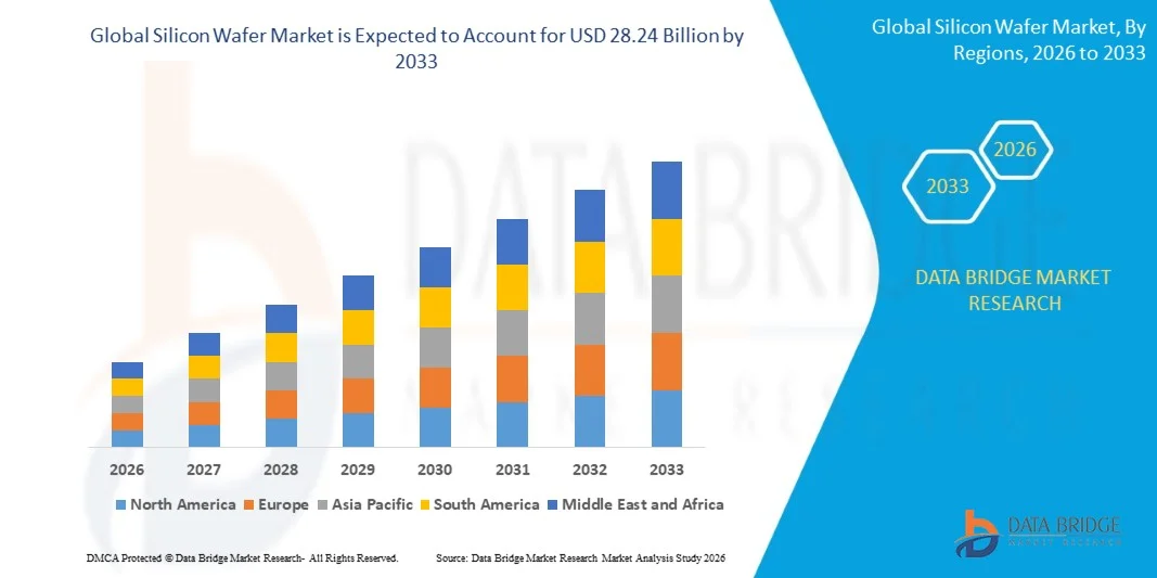
Silicon Wafer Market Size
- The global Silicon Wafer market size was valued at USD 14.49 billion in 2025 and is expected to reach USD 28.24 billion by 2033, at a CAGR of 8.7% during the forecast period 2026 to 2033.
- Market growth is primarily driven by surging demand for advanced semiconductor nodes powering AI processors, 5G chipsets, high-bandwidth memory (HBM), and cloud computing infrastructure, alongside accelerating adoption of electric vehicles (EVs) and IoT devices that require increasingly complex silicon-based components.
- Additionally, massive government-backed semiconductor investment programs including the U.S. CHIPS Act (USD 52.7 billion), the EU Chips Act (EUR 43 billion), and India's semiconductor initiative (INR 91,000 crore) are collectively stimulating domestic wafer supply chain capacity to unprecedented levels, further reinforcing global market expansion.
Silicon Wafer Market Analysis
- Silicon wafers are ultra-pure crystalline substrates – produced through the Czochralski or float zone method and sliced, lapped, polished, and cleaned to nanometer-level tolerances – that serve as the foundational material for virtually all integrated circuits, from microprocessors and memory chips to analog devices, image sensors, and power semiconductors.
- The Silicon Wafer market is witnessing strong momentum from the rapid expansion of artificial intelligence (AI), high-performance computing (HPC), electric vehicles (EVs), 5G infrastructure, and data centers, all of which require advanced semiconductor chips with higher wafer consumption and enhanced fabrication precision.
- Asia-Pacific dominated the Silicon Wafer market with a share of approximately 68.5% in 2025 underpinned by the geographic concentration of tier-1 wafer manufacturers (Shin-Etsu, SUMCO, GlobalWafers), leading foundries (TSMC, Samsung, SMIC), and memory producers (SK Hynix) across Japan, Taiwan, South Korea, and China.
- North America is positioned as the fastest-growing regional market with a CAGR of approximately 10.4% during the forecast period, catalyzed by the CHIPS and Science Act driving over USD 400 million in direct wafer manufacturing grants and supporting nearly USD 4 billion in new domestic semiconductor facility investments.
- The 300 mm wafer segment dominated the market with a share of approximately 41.5%, due to its widespread adoption across leading-edge logic foundries, DRAM manufacturers, NAND flash producers, and advanced packaging facilities. The 300 mm format enables manufacturers to produce significantly more chips per wafer compared to smaller diameters, substantially improving cost-efficiency and yield. Its dominance is reinforced by continuous capacity expansion among top-tier foundries such as TSMC, Samsung, and Intel, all of which are scaling 300 mm wafer starts to meet AI and HPC-driven demand.
Report Scope and Silicon Wafer Market Segmentation
|
Attributes |
Silicon Wafer Key Market Insights |
|
Segments Covered |
|
|
Countries Covered |
North America: • U.S. • Canada • Mexico Europe: • Germany • France • U.K. • Netherlands • Switzerland • Belgium • Russia • Italy • Spain • Turkey • Rest of Europe Asia-Pacific: • China • Japan • India • South Korea • Singapore • Malaysia • Australia • Thailand • Indonesia • Philippines • Rest of Asia-Pacific Middle East and Africa: • Saudi Arabia • U.A.E. • South Africa • Egypt • Israel • Rest of Middle East and Africa South America: • Brazil • Argentina • Rest of South America |
|
Key Market Players |
|
|
Market Opportunities |
|
|
Value Added Data Infosets |
In addition to the insights on market scenarios such as market value, growth rate, segmentation, geographical coverage, and major players, the market reports curated by the Data Bridge Market Research also include in-depth expert analysis, geographically represented company-wise production and capacity, network layouts of distributors and partners, detailed and updated price trend analysis and deficit analysis of supply chain and demand |
Silicon Wafer Market Trends
"Rising AI, HBM, and Advanced Logic Demand Driving 300mm Wafer Growth "
- The global silicon wafer market is entering a prolonged demand supercycle, underpinned by the AI hardware revolution that is creating extraordinary requirements for high-quality 300 mm wafers for advanced logic nodes (below 7 nm), high-bandwidth memory (HBM2E/HBM3), and AI accelerator chips.
- AI and high-performance computing (HPC) wafer demand is growing at an estimated 11.3% CAGR through the forecast period, significantly outpacing overall market growth rates and commanding premium pricing for ultra-flat, ultra-pure substrates meeting sub-angstrom surface roughness specifications.
- Advanced node migration below 7 nm, which captured approximately 24% of market value in 2025, is accelerating the shift to 300 mm wafers across foundries and IDMs, as each transition improves transistor density while requiring stricter defect density and flatness tolerances.
- The structural rise of N-type wafers, growing at approximately 7.2% CAGR driven by solar PV efficiency transitions to TOPCon and HJT cell architectures, is creating diversified revenue streams alongside semiconductor wafer demand.
- Government-driven supply chain nationalization is reshaping the competitive landscape, with the CHIPS Act, EU Chips Act, Japan's RAPIDUS initiative, and India's Semiconductor Mission collectively creating the largest government-funded silicon wafer demand wave in industry history.
- Increasing adoption of chiplet architectures, 2.5D packaging, silicon interposers, and Through-Silicon Via (TSV) technologies is boosting demand for ultra-flat and defect-free wafer substrates with tighter specifications than conventional planar chips.
- The ongoing convergence of advanced manufacturing nodes with expanding application segments – spanning automotive (ADAS, EV powertrains), industrial automation, defense electronics, and telecommunications (5G/6G) – is diversifying the demand base and reducing dependence on any single end market.
Silicon Wafer Market Dynamics
Driver
" AI, EV, and 5G Demand Driving Strong Silicon Wafer Market Growth "
- Explosive growth in AI and machine learning hardware demand – including large language model training chips, inference accelerators, and high-bandwidth memory – is creating sustained and accelerating demand for premium 300 mm silicon wafers produced at advanced nodes.
- The global transition to battery electric vehicles (BEVs) is transforming the automotive semiconductor ecosystem, with each EV integrating up to 3,000 chips including traction inverters, battery management systems, ADAS processors, and power management ICs built on silicon wafer substrates.
- Rapid expansion of 5G infrastructure globally, coupled with early-stage 6G research investments, is driving demand for RF-SOI wafers, GaAs-on-silicon substrates, and advanced analog and mixed-signal devices with stringent purity and resistivity specifications.
- Growing integration of IoT devices across industrial automation, smart cities, and precision agriculture is creating a long-tail demand base for silicon wafers across a wide range of nodes, from advanced sub-7 nm to cost-optimized 28 nm and above.
- Semiconductor content per device continues to increase across virtually all electronic categories, from smartphones and wearables to medical devices and aerospace components, structurally supporting long-term wafer volume demand regardless of unit shipment cycles.
Restraint / Challenge
" Cyclical Demand, Geopolitical Risks, and High Capital Intensity Constraining Market Growth "
- The semiconductor industry's inherent cyclicality poses a persistent risk to silicon wafer demand, as demonstrated by the 2.7% year-on-year decline in global wafer shipments in 2024 caused by inventory corrections in legacy nodes following the post-COVID demand overhang.
- Extreme capital intensity of 300 mm wafer manufacturing – requiring multi-billion-dollar fab investments, ultra-pure chemical processes, and cleanroom environments below ISO Class 1 – creates significant barriers to entry and limits the ability of new competitors to scale rapidly.
- Geopolitical tensions between the U.S. and China over semiconductor technology access, export control restrictions, and wafer equipment sanctions are disrupting established supply chains and compelling costly supply chain redundancy investments across the industry.
- The highly concentrated competitive landscape, with the top five producers (Shin-Etsu, SUMCO, GlobalWafers, Siltronic, SK Siltron) controlling approximately 82–85% of global 300 mm capacity, creates pricing leverage risk for downstream foundries and IDMs with limited alternative sourcing options.
- Transition timelines to 450 mm wafers, while promising long-term cost and yield improvements, face substantial technology and capital barriers, delaying industry-wide adoption and limiting incremental wafer area expansion in the near term.
Silicon Wafer Market Scope
The market is segmented on the basis of wafer size, wafer type, application, and end user.
By Wafer Size
On the basis of Wafer Size, the global Silicon Wafer market is segmented into 150 mm, 200 mm, 300 mm, and Others (including 450 mm).
The 300 mm segment dominated the market with the largest revenue share of approximately 75% in 2025, growing at a CAGR of approximately 9.2%, driven by its widespread adoption across leading-edge logic foundries, DRAM manufacturers, NAND flash producers, and advanced packaging facilities. The 300 mm format enables manufacturers to produce significantly more chips per wafer compared to smaller diameters, substantially improving cost-efficiency and yield. Its dominance is reinforced by continuous capacity expansion among top-tier foundries such as TSMC, Samsung, and Intel, all of which are scaling 300 mm wafer starts to meet AI and HPC-driven demand.
The 450 mm segment (and advanced next-generation formats) is expected to witness the fastest growth rate of approximately 12–15% CAGR during the forecast period, as industry consortia and leading semiconductor manufacturers continue development efforts aimed at commercializing 450 mm production lines. Larger wafer diameters promise further improvements in yield per wafer and production economics, driving active R&D investment by wafer manufacturers and equipment suppliers, particularly for next-generation advanced node applications.
By Wafer Type
On the basis of Wafer Type, the global Silicon Wafer market is segmented into Polished Wafers, Epitaxial Wafers, SOI Wafers, and Diffused Wafers.
The Polished (Prime) Wafers segment dominated the market with a share of approximately 73.7% in 2025 and a CAGR of approximately 7.8%, serving as the foundational substrate for the vast majority of integrated circuit manufacturing across memory, logic, analog, and mixed-signal applications. Prime polished wafers undergo stringent surface finishing processes to achieve the mirror-like flatness required by advanced photolithography, making them indispensable for sub-10 nm node production at leading foundries globally.
The Silicon-on-Insulator (SOI) Wafers segment is expected to witness the fastest growth at a CAGR of approximately 11.5% during the forecast period, driven by accelerating demand for RF-SOI substrates in 5G radio frequency front-end modules, fully-depleted SOI (FDSOI) wafers for low-power automotive and IoT applications, and ultra-high-resistivity SOI grades for advanced RF and mmWave applications. Growing adoption of SOI technology in power electronics, analog ICs, and next-generation CMOS devices is reinforcing rapid segment expansion.
By Application
On the basis of Application, the global Silicon Wafer market is segmented into Consumer Electronics, Automotive, Industrial, Telecommunications, Solar Cells, and Others.
The Consumer Electronics segment dominated the market with a share of approximately 41.5% in 2025 and a CAGR of approximately 7.2%, driven by persistent and large-scale demand for silicon wafers used in smartphone application processors, mobile DRAM and NAND flash, display driver ICs, image sensors, and wearable semiconductor components. Integrated circuits for consumer electronics span the full spectrum of silicon wafer applications, from advanced sub-3 nm logic nodes in flagship mobile processors to mature nodes in analog and power management devices, sustaining broad-based wafer demand across multiple diameter and type categories.
The Automotive segment is expected to witness the fastest growth at a CAGR of approximately 8.3% during the forecast period, fueled by rapid electrification of passenger and commercial vehicles, proliferation of ADAS sensors and processors, and mandatory integration of domain-controller and zonal-architecture semiconductor systems in next-generation vehicles. Each battery electric vehicle integrates up to 3,000 semiconductor chips across traction inverters, battery management systems, onboard chargers, V2X communication modules, and advanced driver assistance processors, translating into 15–20 times greater semiconductor content per vehicle compared to a conventional internal combustion engine automobile.
By End User
On the basis of End User, the global Silicon Wafer market is segmented into Foundries, Integrated Device Manufacturers (IDMs), and Others.
The Foundries segment dominated the market with the largest revenue share of approximately 55%+ in 2025 and a CAGR of approximately 8.5%, driven by the outsized wafer consumption of pure-play foundries such as TSMC, Samsung Foundry, and SMIC, which collectively account for the majority of advanced and mature node wafer starts globally. The fabless semiconductor model – where chip designers like Apple, Qualcomm, NVIDIA, and AMD rely entirely on foundry wafer services – continues to concentrate wafer demand at leading foundry customers, reinforcing the segment's dominant position in the silicon wafer supply chain.
The IDM (Integrated Device Manufacturers) segment focused on automotive and power applications is expected to witness the fastest growth at a CAGR of approximately 9.8% during the forecast period, as companies such as Infineon, STMicroelectronics, ON Semiconductor, and Texas Instruments rapidly expand their 200 mm and 300 mm in-house wafer production for power semiconductors, silicon carbide (SiC) devices, and automotive-grade analog ICs. Growing self-sufficiency drives among leading IDMs, supported by government incentives and supply chain resilience mandates, is accelerating wafer capacity investments within this segment.
Silicon Wafer Market Regional Analysis
- Asia-Pacific dominated the Silicon Wafer market with the largest revenue share of approximately 68.5% in 2025 and a CAGR of approximately 8.2%, anchored by Japan's Shin-Etsu Chemical and SUMCO Corporation as the world's top two silicon wafer producers, Taiwan's extraordinary concentration of leading foundry demand from TSMC and GlobalWafers, and South Korea's Samsung Electronics and SK Hynix as the world's largest DRAM and NAND memory producers. China's rapidly expanding domestic wafer manufacturing capabilities, led by National Silicon Industry Group (NSIG) and Zhonghuan Advanced Semiconductor Materials, are further solidifying the region's leadership position.
- Industries across the region benefit from decades of accumulated semiconductor manufacturing expertise, world-class supplier ecosystems, and government support programs that collectively create an unparalleled competitive advantage in silicon wafer production and consumption.
- Asia-Pacific's dominant position is further reinforced by the region's role as the primary manufacturing hub for consumer electronics – including smartphones, PCs, and tablets – which collectively represent the single largest end-use category for silicon wafers globally.
U.S. Silicon Wafer Market Insight
The U.S. Silicon Wafer market holds a commanding position in North America, driven by the highest concentration of semiconductor R&D activity, the presence of leading fabless chip designers (NVIDIA, AMD, Qualcomm, Apple), and the rapid build-out of domestic advanced manufacturing capacity under the CHIPS and Science Act. The U.S. government's USD 406 million grant to GlobalWafers for 300 mm wafer production, supporting nearly USD 4 billion in total facility investment and creating over 2,580 jobs, exemplifies the structural investment being made in domestic silicon wafer supply chains. Growing demand for AI data center chips, defense-grade semiconductors, and advanced automotive electronics is reinforcing U.S. market expansion through 2033.
Europe Silicon Wafer Market Insight
The Europe Silicon Wafer market is experiencing steady growth, driven by strong demand from Germany, France, the Netherlands, and Switzerland, where advanced semiconductor capabilities are anchored by Siltronic AG's world-class 300 mm polished and epitaxial wafer production and Soitec's leadership in SOI wafer technology. The EU Chips Act's EUR 43 billion investment framework is catalyzing new semiconductor manufacturing investments across the continent, supporting the development of a more resilient European chip supply chain. Growing EV production, renewable energy infrastructure, and industrial automation are driving silicon wafer demand across European end markets.
Germany Silicon Wafer Market Insight
The Germany Silicon Wafer market is expected to grow steadily during the forecast period, underpinned by Germany's exceptional strength in industrial and automotive electronics manufacturing. Rising demand from the automotive sector for EV power modules, ADAS systems, and embedded controllers is driving significant silicon wafer consumption among Germany's tier-1 automotive semiconductor customers including Infineon Technologies, Robert Bosch, and Continental. Germany's strong engineering ecosystem, proximity to Siltronic AG's production base, and participation in EU-level semiconductor investment programs are supporting the country's mid-term wafer demand trajectory.
Japan Silicon Wafer Market Insight
Japan holds a uniquely central position in the global Silicon Wafer market as the home of Shin-Etsu Chemical and SUMCO Corporation, the world's #1 and #2 silicon wafer producers, which together account for a substantial portion of global 300 mm wafer capacity. Japan's government-backed semiconductor revival strategy, including the RAPIDUS initiative targeting 2 nm logic production and substantial investment in Kumamoto-based TSMC fabrication facilities, is reinforcing Japan's strategic importance in the global silicon wafer supply chain. Japan's aging population and advanced manufacturing ethos continue to support sustained investment in semiconductor technology innovation.
China Silicon Wafer Market Insight
China is expected to witness the highest CAGR among individual countries in the global Silicon Wafer market, driven by Beijing's aggressive Healthy China 2030 and semiconductor self-sufficiency strategies that are directing hundreds of billions of renminbi toward domestic wafer manufacturing capacity. National Silicon Industry Group (NSIG) and Zhonghuan Advanced Semiconductor Materials are rapidly scaling 300 mm wafer production capabilities to reduce dependence on Japanese and Taiwanese suppliers. Growing domestic demand from SMIC, Huahong Group, and numerous Chinese fabless companies, combined with government procurement mandates favoring domestic semiconductor supply chains, are creating a powerful secular growth driver for China's silicon wafer market.
India Silicon Wafer Market Insight
The India Silicon Wafer market is at an early but rapidly accelerating stage of development, catalyzed by India's INR 91,000 crore Semiconductor Mission and the establishment of Tata Electronics' semiconductor manufacturing facility in partnership with PSMC of Taiwan, and CG Power's ATMP facility. Growing demand for consumer electronics, telecommunications infrastructure expansion under 5G rollout, and India's ambition to become a significant global semiconductor manufacturing hub are creating new domestic silicon wafer consumption channels. India's expanding electronics manufacturing ecosystem, supported by PLI incentives, is expected to drive sustained silicon wafer demand growth through 2033.
Silicon Wafer Market Share
The Silicon Wafer industry is primarily led by well-established, highly specialized companies, including:
- Shin-Etsu Chemical Co., Ltd. (Japan)
- SUMCO Corporation (Japan)
- GlobalWafers Co., Ltd. (Taiwan)
- Siltronic AG (Germany)
- SK Siltron Co., Ltd. (South Korea)
- Soitec SA (France)
- National Silicon Industry Group – NSIG (China)
- Zhonghuan Advanced Semiconductor Materials Co., Ltd. (China)
- Wafer Works Corporation (Taiwan)
- Okmetic Inc. (Finland)
- FST Corporation (Taiwan)
- Silicon Materials Inc. (US)
Latest Developments in the Global Silicon Wafer Market
- In October 2025, Samsung Electronics (South Korea) announced plans to invest USD 10 billion in expanding its semiconductor manufacturing facilities in the United States, bolstering 300 mm wafer production capabilities to meet surging domestic demand for advanced chips in automotive and IoT sectors.
- In September 2025, GlobalFoundries (US) launched a new line of silicon wafers optimized for advanced power electronics and automotive-grade semiconductor devices, targeting the rapidly growing EV and industrial automation markets.
- In November 2025, Intel Corporation (US) announced a strategic partnership with a leading AI firm to integrate AI-driven analytics into its wafer fabrication processes, targeting improved yield rates and reduced operational costs through machine learning optimization of defect detection.
- In 2025–2026, GlobalWafers received a USD 406 million U.S. government grant under the CHIPS and Science Act for 300 mm wafer production in Sherman, Texas, supporting nearly USD 4 billion in total facility investment and creating over 1,700 construction and 880 manufacturing jobs.
- In 2026, Shin-Etsu Chemical announced continued capacity expansion of its 300 mm polished and epitaxial wafer production lines in Japan and the U.S. to accommodate growing AI chip and advanced logic node demand from foundry customers.
SKU-
- Interactive Data Analysis Dashboard
- Company Analysis Dashboard for high growth potential opportunities
- Research Analyst Access for customization & queries
- Competitor Analysis with Interactive dashboard
- Latest News, Updates & Trend analysis
- Harness the Power of Benchmark Analysis for Comprehensive Competitor Tracking
Global Silicon Wafer Market, Supply Chain Analysis and Ecosystem Framework
To support market growth and help clients navigate the impact of geopolitical shifts, DBMR has integrated in-depth supply chain analysis into its Global Silicon Wafer Market research reports. This addition empowers clients to respond effectively to global changes affecting their industries. The supply chain analysis section includes detailed insights such as Global Silicon Wafer Market consumption and production by country, price trend analysis, the impact of tariffs and geopolitical developments, and import and export trends by country and HSN code. It also highlights major suppliers with data on production capacity and company profiles, as well as key importers and exporters. In addition to research, DBMR offers specialized supply chain consulting services backed by over a decade of experience, providing solutions like supplier discovery, supplier risk assessment, price trend analysis, impact evaluation of inflation and trade route changes, and comprehensive market trend analysis.
Data collection and base year analysis are done using data collection modules with large sample sizes. The stage includes obtaining market information or related data through various sources and strategies. It includes examining and planning all the data acquired from the past in advance. It likewise envelops the examination of information inconsistencies seen across different information sources. The market data is analysed and estimated using market statistical and coherent models. Also, market share analysis and key trend analysis are the major success factors in the market report. To know more, please request an analyst call or drop down your inquiry.
The key research methodology used by DBMR research team is data triangulation which involves data mining, analysis of the impact of data variables on the market and primary (industry expert) validation. Data models include Vendor Positioning Grid, Market Time Line Analysis, Market Overview and Guide, Company Positioning Grid, Patent Analysis, Pricing Analysis, Company Market Share Analysis, Standards of Measurement, Global versus Regional and Vendor Share Analysis. To know more about the research methodology, drop in an inquiry to speak to our industry experts.
Data Bridge Market Research is a leader in advanced formative research. We take pride in servicing our existing and new customers with data and analysis that match and suits their goal. The report can be customized to include price trend analysis of target brands understanding the market for additional countries (ask for the list of countries), clinical trial results data, literature review, refurbished market and product base analysis. Market analysis of target competitors can be analyzed from technology-based analysis to market portfolio strategies. We can add as many competitors that you require data about in the format and data style you are looking for. Our team of analysts can also provide you data in crude raw excel files pivot tables (Fact book) or can assist you in creating presentations from the data sets available in the report.


