

What is the Surface Inspection Market Size and Growth Rate?
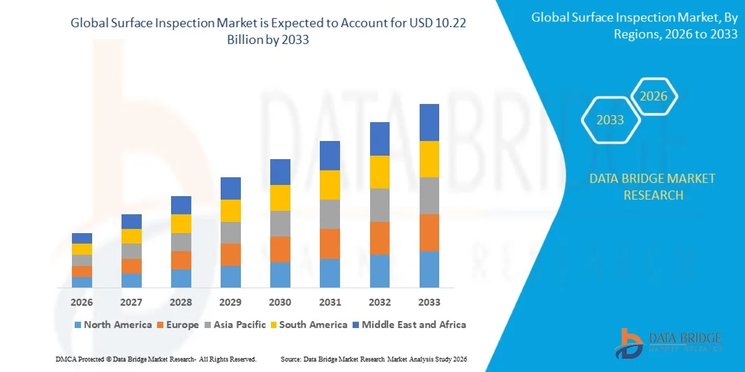
- As per Data Bridge Market Research analysis, the surface inspection market was valued at USD 5.25 billion in 2025 and is projected to reach USD 10.22 billion by 2033, growing at a CAGR of 8.68% from 2026 to 2033.
- The market is experiencing steady growth driven by the rapid expansion of global semiconductor fabrication capacity, increasing miniaturization of electronic components requiring higher-precision defect detection, and growing integration of artificial intelligence and deep learning algorithms into inspection systems to improve defect classification accuracy and reduce false rejection rates.
- The growing emphasis on zero-defect manufacturing, yield optimization, and reduced production waste is compelling semiconductor fabs, display manufacturers, and electronics assemblers to invest in advanced automated surface inspection systems. AI-based inspection platforms are increasingly complementing and, in some applications, replacing traditional rule-based machine vision systems, offering improved defect classification accuracy and reduced manual review requirements.
- The convergence of surface inspection technology with broader manufacturing execution and yield management systems is enabling fabs and electronics assemblers to correlate defect data directly with upstream process parameters, supporting faster root-cause identification and continuous process improvement across production lines.
Market Size & Forecast
- Global Market Value (2025): USD 5.25 Billion
- Expected Market Value (2033): USD 10.22 Billion
- Forecast CAGR (2026–2033): 8.68%
What are the Major Takeaways of the Surface Inspection Market?
- Asia-Pacific dominated the global surface inspection market with the largest revenue share of 42.36% in 2025, supported by the region’s concentration of semiconductor fabrication facilities, extensive electronics manufacturing infrastructure, and significant investment in fab capacity expansion across Taiwan, South Korea, China, and Japan.
- North America is expected to be the fastest-growing region at a CAGR of 10.4% from 2026 to 2033, fueled by accelerating domestic semiconductor fab construction under national manufacturing incentive programs and rapid adoption of AI-based inspection technology.
- The hardware component segment led the market with a 54.28% share in 2025, driven by continued demand for high-resolution cameras, precision optics, and advanced lighting systems essential to accurate defect detection across diverse surface types.
- The AI/deep learning-based inspection technology segment is the fastest-growing category, projected to register a CAGR of 11.6%, reflecting rapid adoption of machine learning algorithms capable of identifying subtle and previously undetectable defect patterns.
- The semiconductor wafer inspection application segment dominated the application category with a 36.74% revenue share in 2025, led by the critical importance of defect detection in maintaining high yields across increasingly complex, miniaturized chip fabrication processes.
- Inline/on-production-line inspection deployment accounted for 61.83% of the market share in 2025, preferred due to its ability to identify defects in real time without disrupting continuous manufacturing flow.
- The flat panel display inspection application segment is the fastest-growing category, with a CAGR of 10.1%, driven by rising production of high-resolution OLED and microLED displays requiring increasingly precise defect detection capabilities.
Report Scope and Surface Inspection Market Segmentation
|
Attributes |
Surface Inspection Key Market Insights |
|
Segments Covered |
|
|
Countries Covered |
North America
Europe
Asia-Pacific
Middle East and Africa
South America
|
|
Key Market Players |
|
|
Market Opportunities |
|
|
Value Added Data Infosets |
In addition to the insights on market scenarios such as market value, growth rate, segmentation, geographical coverage, and major players, the market reports curated by the Data Bridge Market Research also include in-depth expert analysis, geographically represented company-wise production and capacity, network layouts of distributors and partners, detailed and updated price trend analysis and deficit analysis of supply chain and demand. |
What is the Key Trend in the Surface Inspection Market?
- Semiconductor and electronics manufacturers are increasingly deploying deep learning-based inspection systems capable of continuously improving defect classification accuracy through training on newly acquired defect data, reducing reliance on manually programmed, rule-based detection logic.
- For instance, in February 2025, Applied Materials introduced the SEMVision H20 defect review system, which combines advanced eBeam imaging with deep-learning AI models trained using semiconductor fab data to distinguish true defects from nuisance defects and improve automated defect classification.
- Growing integration of hyperspectral and advanced spectral imaging technologies into surface inspection systems is enabling manufacturers to identify surface deviations, contamination, material variations, and defects in deeper wafer layers that may not be detectable through conventional visible-light imaging.
- For instance, in July 2025, Fraunhofer IPMS and DIVE imaging systems GmbH reported the deployment of the VEpioneer hyperspectral inspection system, which combines spectroscopy, imaging, and AI-based image analysis to identify surface deviations, contamination, and defects in deeper wafer layers.
- Equipment manufacturers are increasingly developing modular and scalable inspection platforms that allow semiconductor fabs and electronics manufacturers to incrementally expand inspection capabilities as production volumes, product mix, and defect detection requirements evolve.
- For instance, in February 2025, Saki Corporation launched its 3Si/3Di-EX Series, featuring a modular hardware architecture that allows optical units to be upgraded without replacing the entire inspection platform, enabling manufacturers to expand inspection capabilities as manufacturing requirements change.
- Inspection system developers are increasingly incorporating advanced optical techniques to detect internal and subsurface defects in semiconductor and advanced-packaging materials, expanding inspection beyond conventional surface-visible defects.
- For instance, in February 2025, TASMIT Inc. launched an INSPECTRA inspection system for large glass substrates used in advanced semiconductor packaging, capable of inspecting front and back surfaces as well as internal defects using polarized-light optical inspection and a dedicated defect-detection algorithm.
- As semiconductor fabs, advanced-packaging manufacturers, display producers, and electronics assemblers continue to prioritize yield optimization, defect traceability, early defect detection, and inspection throughput, the adoption of AI-enabled, spectral, modular, and high-resolution surface inspection technologies is expected to accelerate, reinforcing their role in modern electronics manufacturing quality control.
What are the Key Drivers of the Surface Inspection Market?
- The rapid expansion of global semiconductor fabrication and advanced packaging capacity, driven by rising demand for high-performance computing, artificial intelligence, automotive, and consumer electronics applications, is increasing demand for high-precision surface inspection and metrology systems capable of maintaining manufacturing yield across increasingly complex production processes.
- For instance, in April 2025, Applied Materials announced a strategic investment in BE Semiconductor Industries (BESI) and extended their collaboration on hybrid-bonding equipment for advanced semiconductor packaging, reflecting increasing industry investment in equipment technologies required for higher-density chiplet and advanced-packaging manufacturing.
- The continued miniaturization of semiconductor devices and increasing adoption of advanced packaging technologies such as high-bandwidth memory (HBM), chiplets, and hybrid bonding are driving demand for inspection systems capable of detecting increasingly small and subtle defects that can affect device performance and yield.
- For instance, in November 2024, Camtek announced more than $50 million in initial orders for its Hawk inspection and metrology platform, designed for advanced packaging applications including HBM, chiplets, and hybrid bonding, with deliveries scheduled throughout 2025.
- The growing global emphasis on domestic semiconductor supply-chain resilience, supported by government incentives and strategic industrial policies, is prompting substantial investment in new semiconductor manufacturing facilities and equipment, creating additional demand for inspection and metrology systems.
- For instance, in October 2024, the U.S. Department of the Treasury and Internal Revenue Service released final rules for the Advanced Manufacturing Investment Credit under the CHIPS and Science Act, providing greater certainty for investments in U.S. semiconductor manufacturing facilities and semiconductor manufacturing equipment.
Which Factors are Challenging the Growth of the Surface Inspection Market?
- Advanced surface inspection systems, particularly those incorporating AI-based defect classification, high-resolution imaging, and automated data analysis, require substantial investment in inspection hardware, computing infrastructure, software, and data management. These high implementation costs can limit adoption among smaller manufacturers and facilities operating cost-sensitive or legacy production lines.
- For instance, in February 2025, Onto Innovation reported continued customer investment in advanced 2D inspection and 3D metrology systems to support high-bandwidth-memory manufacturing, highlighting the significant capital requirements associated with increasingly sophisticated semiconductor inspection technologies.
- A shortage of personnel with combined expertise in semiconductor manufacturing, machine vision, artificial intelligence, and advanced packaging is constraining manufacturers' ability to implement and operate increasingly sophisticated inspection technologies.
- For instance, in April 2024, SK hynix announced plans for a $3.9 billion advanced packaging facility in Indiana and highlighted the need for several hundred engineers with expertise across physics, chemistry, materials science, and electronics engineering, demonstrating the significant specialized workforce requirements associated with advanced semiconductor manufacturing.
- Therefore, high investment costs and a shortage of skilled professionals are key challenges to surface inspection market growth, particularly for smaller manufacturers and legacy production facilities, potentially slowing adoption of advanced inspection technologies.
How is the Surface Inspection Market Segmented?
The surface inspection market is segmented on the basis of component, technology, application, end user, deployment, and defect type detected.
- By Component
On the basis of component, the global surface inspection market is segmented into hardware, software, and services. The hardware segment dominated the market with a 54.28% share in 2025, owing to continued demand for high-resolution cameras, precision optics, and advanced lighting systems essential to accurate defect detection across diverse surface types. These components remain foundational to inspection system performance regardless of the sophistication of the underlying image processing software.
The software segment is projected to register the fastest growth at a CAGR of 10.8% from 2026 to 2033, driven by rising adoption of AI-based image processing and defect classification algorithms that continuously improve inspection accuracy through machine learning. Growing demand for cloud-based inspection data analytics platforms is further accelerating segment expansion.
- By Technology
On the basis of technology, the global surface inspection market is segmented into machine vision-based inspection, laser-based inspection, X-ray inspection, ultrasonic inspection, and AI/deep learning-based inspection. The machine vision-based inspection segment led the market with a 41.62% share in 2025, supported by its widespread use across a broad range of surface inspection applications and well-established integration with existing production line automation systems.
The AI/deep learning-based inspection segment is expected to experience the fastest growth at a CAGR of 11.6% from 2026 to 2033, driven by rapid adoption of machine learning algorithms capable of identifying subtle and previously undetectable defect patterns while continuously improving classification accuracy through ongoing training.
- By Application
On the basis of application, the global surface inspection market is segmented into semiconductor wafer inspection, flat panel display inspection, PCB inspection, metal surface inspection, glass & ceramics inspection, automotive component inspection, and others. The semiconductor wafer inspection segment dominated the market with a share of 36.74% in 2025 due to the critical importance of defect detection in maintaining high yields across increasingly complex, miniaturized chip fabrication processes. the continued global expansion of semiconductor fabrication capacity is reinforcing the dominance of this segment.
The flat panel display inspection segment is expected to witness the fastest CAGR of 10.1% from 2026 to 2033, driven by this growth is fueled by rising production of high-resolution OLED and microLED displays requiring increasingly precise defect detection capabilities to maintain acceptable yield rates across large-panel manufacturing processes.
- By End User
On the basis of end user, the global surface inspection market is segmented into semiconductor & electronics manufacturers, automotive industry, metal & machinery manufacturing, glass & ceramics industry, and others. The semiconductor & electronics manufacturers segment dominated the market with a share of 48.37% in 2025 due to the industry’s stringent quality requirements and continuous investment in advanced inspection technology to support high-yield, high-volume chip and component production. the widespread adoption of automated inspection across every stage of semiconductor manufacturing is reinforcing this segment’s leading position.
The automotive industry segment is expected to witness the fastest CAGR of 9.8% from 2026 to 2033, driven by rising integration of advanced electronic components and power semiconductor devices in electric and autonomous vehicles, requiring stringent surface inspection to ensure component reliability and safety compliance.
- By Deployment
On the basis of deployment, the global surface inspection market is segmented into inline/on-production-line inspection and offline/standalone inspection. The inline/on-production-line inspection segment dominated the market with a share of 61.83% in 2025 due to its ability to identify defects in real time without disrupting continuous manufacturing flow, enabling immediate corrective action and reducing downstream waste. increasing manufacturing automation and just-in-time production practices continue to reinforce this segment’s leading position.
The offline/standalone inspection segment is expected to witness the fastest CAGR of 9.2% from 2026 to 2033, driven by rising demand for detailed, high-resolution failure analysis and root-cause investigation capabilities that complement inline inspection systems for complex defect characterization requiring specialized equipment not suited to production-line integration.
- By Defect Type Detected
On the basis of defect type detected, the global surface inspection market is segmented into scratches & cracks, particle contamination, discoloration/stains, dimensional defects, and others. The particle contamination segment dominated the market with a share of 33.42% in 2025 due to its critical importance in semiconductor and electronics manufacturing, where even microscopic particle contamination can cause significant yield loss and device failure. stringent cleanroom and contamination control requirements across the industry continue to support strong demand for particle detection capabilities.
The dimensional defects segment is expected to witness the fastest CAGR of 9.6% from 2026 to 2033, driven by increasing miniaturization of electronic components requiring progressively more precise dimensional measurement and defect detection capabilities to maintain manufacturing tolerances.
Which Region Holds the Largest Share of the Surface Inspection Market?
- Asia-Pacific dominated the surface inspection market and accounted for the largest revenue share of 42.36% in 2025, supported by the region’s concentration of semiconductor fabrication facilities, extensive electronics manufacturing infrastructure, and significant investment in fab capacity expansion across the region.
- The region also benefits from a dense concentration of semiconductor foundries, display panel manufacturers, and electronics assembly operations, along with strong government support for domestic semiconductor industry development. Continued fab capacity expansion across multiple countries continues to strengthen Asia-Pacific’s leadership position in the global market.
China Surface Inspection Market Insight
The China surface inspection market is growing rapidly, driven by extensive domestic semiconductor fabrication capacity expansion, rising government investment in achieving semiconductor manufacturing self-sufficiency, and growing electronics assembly and display manufacturing infrastructure. Growing adoption of both domestic and international inspection technology across expanding fab capacity is significantly boosting market demand. In addition, rising domestic inspection equipment manufacturing capabilities are positioning China as one of the fastest-growing markets for surface inspection technology globally.
Japan Surface Inspection Market Insight
The Japan surface inspection market is witnessing consistent growth due to the country’s strong semiconductor equipment manufacturing base, advanced machine vision technology development capabilities, and continuous investment in precision electronics manufacturing. Leading Japanese equipment manufacturers continue to develop innovative inspection technologies for both domestic and export markets. Moreover, continued innovation in high-precision optical and sensor technology is further contributing to market growth in Japan.
Europe Surface Inspection Market Insight
The growth of the Europe surface inspection market is heavily propelled by the rapid adoption of Industry 4.0 and automated manufacturing technologies, as regional factories integrate vision systems to maximize yield. Furthermore, strict European regulatory mandates across critical sectors like electronics and pharmaceuticals demand flawless quality control, prompting companies to deploy advanced inspection setups. The integration of artificial intelligence and deep learning with traditional camera systems significantly boosts defect detection accuracy. Additionally, rising labor costs and the push to reduce material waste across Germany, France, and Italy continue to accelerate regional demand for automated surface verification.
Germany Surface Inspection Market Insight
The Germany surface inspection market is expanding steadily, supported by the country’s strong industrial automation and machine vision technology sector, advanced automotive manufacturing base, and increasing adoption of inspection technology across metal and glass manufacturing industries. Leading European machine vision companies headquartered in the region continue to invest in advanced inspection algorithm development. Continued focus on Industry 4.0 integration and manufacturing quality control is further driving market growth in Germany.
U.K. Surface Inspection Market Insight
The U.K. surface inspection market is expanding steadily, driven by the acceleration of smart manufacturing, stringent quality control regulations, and labor optimization across automotive, aerospace, electronics, and metals industries. Driven by widespread industrial automation, companies are increasingly deploying AI-powered computer and 3D vision systems to eliminate manual inspection errors. High-resolution cameras and machine learning software enable real-time defect detection, ensuring precise compliance, minimizing waste, and boosting production yield across high-precision British manufacturing sectors.
Which are the Top Companies in Surface Inspection Market?
The surface inspection industry is primarily led by well-established companies, including:
- KLA Corporation (U.S.)
- Applied Materials, Inc. (U.S.)
- Hitachi High-Tech Corporation (Japan)
- Camtek Ltd. (Israel)
- Onto Innovation Inc. (U.S.)
- Cognex Corporation (U.S.)
- ISRA VISION AG (Atlas Copco) (Germany)
- Basler AG (Germany)
- Keyence Corporation (Japan)
- Omron Corporation (Japan)
- Teledyne DALSA (Teledyne Technologies) (Canada)
- Advantest Corporation (Japan)
- Nordson Corporation (U.S.)
- National Instruments (Emerson) (U.S.)
- Mitsubishi Electric Corporation (Japan)
- Toray Engineering Co., Ltd. (Japan)
- Baumer Group (Switzerland)
- Vitronic GmbH (Germany)
- SICK AG (Germany)
- Zebra Technologies Corporation (U.S.)
What are Latest Developments in Surface Inspection Market?
- In September 2025, KLA Corporation launched a next-generation wafer inspection system featuring enhanced AI-based defect classification capabilities, enabling semiconductor fabs to detect increasingly subtle yield-impacting defects across advanced process nodes.
- In January 2025, Camtek expanded its manufacturing facility in Asia-Pacific to increase production capacity for its advanced packaging inspection systems, meeting rising regional demand from fabs transitioning to more complex chip packaging architectures.
- In November 2025, ISRA VISION introduced an upgraded surface inspection platform for flat panel display manufacturing, featuring improved hyperspectral imaging capabilities for detecting subsurface defects in large-format OLED panels.
- In November 2024, Cognex launched a new deep learning-based inspection software suite designed to reduce the time and expertise required to deploy AI-based defect detection across diverse manufacturing applications.
- In June 2023, Hitachi High-Tech partnered with several semiconductor fabs in Asia-Pacific to conduct field validation of its advanced wafer defect review systems, demonstrating improved defect classification accuracy across multiple advanced process node applications.
- In August 2024, Onto Innovation expanded its manufacturing capacity for advanced packaging metrology and inspection systems to meet rising demand from semiconductor companies transitioning to next-generation chip packaging technologies.
- Interactive Data Analysis Dashboard
- Company Analysis Dashboard for high growth potential opportunities
- Research Analyst Access for customization & queries
- Competitor Analysis with Interactive dashboard
- Latest News, Updates & Trend analysis
- Harness the Power of Benchmark Analysis for Comprehensive Competitor Tracking
Global Surface Inspection Market, Supply Chain Analysis and Ecosystem Framework
To support market growth and help clients navigate the impact of geopolitical shifts, DBMR has integrated in-depth supply chain analysis into its Global Surface Inspection Market research reports. This addition empowers clients to respond effectively to global changes affecting their industries. The supply chain analysis section includes detailed insights such as Global Surface Inspection Market consumption and production by country, price trend analysis, the impact of tariffs and geopolitical developments, and import and export trends by country and HSN code. It also highlights major suppliers with data on production capacity and company profiles, as well as key importers and exporters. In addition to research, DBMR offers specialized supply chain consulting services backed by over a decade of experience, providing solutions like supplier discovery, supplier risk assessment, price trend analysis, impact evaluation of inflation and trade route changes, and comprehensive market trend analysis.
Data collection and base year analysis are done using data collection modules with large sample sizes. The stage includes obtaining market information or related data through various sources and strategies. It includes examining and planning all the data acquired from the past in advance. It likewise envelops the examination of information inconsistencies seen across different information sources. The market data is analysed and estimated using market statistical and coherent models. Also, market share analysis and key trend analysis are the major success factors in the market report. To know more, please request an analyst call or drop down your inquiry.
The key research methodology used by DBMR research team is data triangulation which involves data mining, analysis of the impact of data variables on the market and primary (industry expert) validation. Data models include Vendor Positioning Grid, Market Time Line Analysis, Market Overview and Guide, Company Positioning Grid, Patent Analysis, Pricing Analysis, Company Market Share Analysis, Standards of Measurement, Global versus Regional and Vendor Share Analysis. To know more about the research methodology, drop in an inquiry to speak to our industry experts.
Data Bridge Market Research is a leader in advanced formative research. We take pride in servicing our existing and new customers with data and analysis that match and suits their goal. The report can be customized to include price trend analysis of target brands understanding the market for additional countries (ask for the list of countries), clinical trial results data, literature review, refurbished market and product base analysis. Market analysis of target competitors can be analyzed from technology-based analysis to market portfolio strategies. We can add as many competitors that you require data about in the format and data style you are looking for. Our team of analysts can also provide you data in crude raw excel files pivot tables (Fact book) or can assist you in creating presentations from the data sets available in the report.