

What is the Thin and Ultra-Thin Films Market Size and Growth Rate?
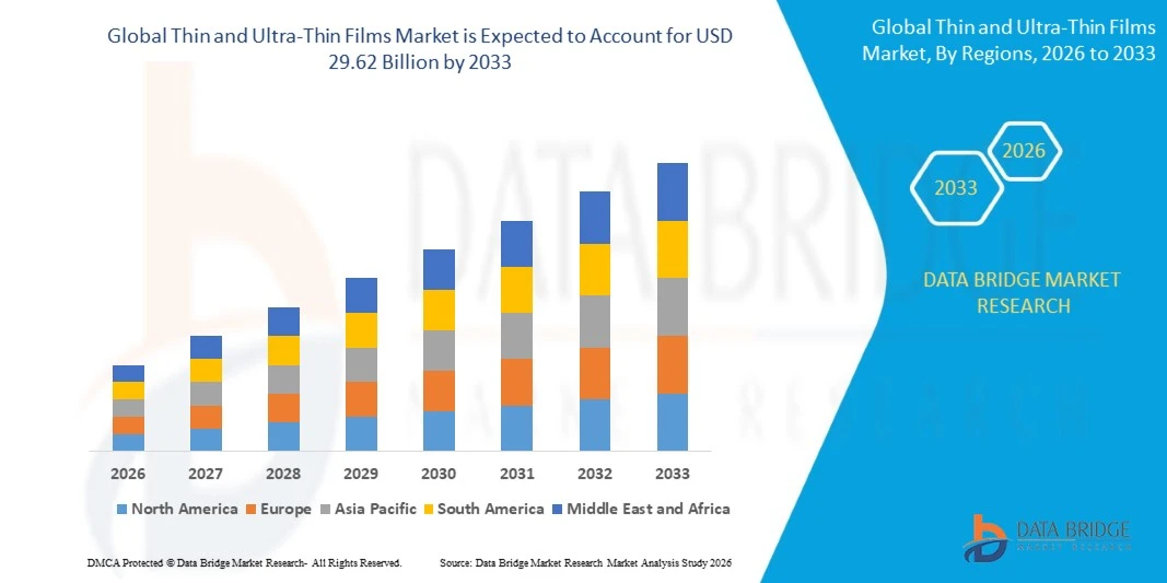
- As per Data Bridge Market Research analysis, the thin and ultra-thin films market was valued at USD 9.42 billion in 2025 and is projected to reach USD 29.62 billion by 2033, growing at a CAGR of 15.40% from 2026 to 2033.
- The market is experiencing consistent growth driven by rising demand for miniaturized electronic components, rapid advancements in thin-film deposition technologies, and expanding applications across semiconductors, solar panels, medical devices, and automotive electronics.
- The increasing adoption of flexible electronics globally, combined with growing investments in renewable energy and advanced semiconductor manufacturing, is encouraging manufacturers to develop high-performance thin and ultra-thin films. Physical vapor deposition and chemical vapor deposition technologies are supporting the production of uniform, durable, and precisely engineered coatings, offering improved electrical performance, energy efficiency, and material utilization across various industries.
Market Size & Forecast
- Global Market Value (2025): USD 9.42 Billion
- Expected Market Value (2033): USD 29.62 Billion
- Forecast CAGR (2026–2033): 15.40%
- Leading Region in 2025: North America
- Fastest Growing Region: Asia Pacific
What are the Major Takeaways of the Thin and Ultra-Thin Films Market?
- North America dominated the thin and ultra-thin films market with the largest revenue share of 36.5% in 2025, supported by advanced semiconductor manufacturing infrastructure, strong research and development investments, and growing demand for high-performance electronic materials.
- Asia-Pacific is expected to be the fastest-growing region at a CAGR of 16.4% from 2026 to 2033, fueled by expanding semiconductor production, rapid industrialization, increasing solar energy investments, and rising electronics demand in China, Japan, South Korea, and India.
- The gaseous state segment led the market with a 45.2% share in 2025, driven by the extensive use of vapor-based coating processes in semiconductor manufacturing, optical coatings, and advanced electronic components.
- Solutions state are the fastest-growing coating methods type, projected to register a CAGR of 18.7%, reflecting the surge in demand for cost-effective coating methods and scalable manufacturing processes.
- The thin segment dominated the type category with a 60.0% revenue share in 2025, led by its extensive applications across semiconductors, consumer electronics, optical components, and renewable energy systems
- Physical deposition accounted for 36.2% of the market share in 2025, preferred by its extensive use in semiconductor manufacturing, optical coatings, and industrial surface treatments.
- The healthcare and biomedical applications segment is the fastest-growing application category, with a CAGR of 13.8%, driven by increasing demand for biocompatible coatings, implantable electronics, diagnostic devices, and advanced medical technologies.
Report Scope and Thin and Ultra-Thin Films Market Segmentation
|
Attributes |
Thin and Ultra-Thin Films Key Market Insights |
|
Segments Covered |
|
|
Countries Covered |
North America
Europe
Asia-Pacific
Middle East and Africa
South America
|
|
Key Market Players |
|
|
Market Opportunities |
|
|
Value Added Data Infosets |
In addition to the insights on market scenarios such as market value, growth rate, segmentation, geographical coverage, and major players, the market reports curated by the Data Bridge Market Research also include in-depth expert analysis, geographically represented company-wise production and capacity, network layouts of distributors and partners, detailed and updated price trend analysis and deficit analysis of supply chain and demand. |
What is the Key Trend in the Thin and Ultra-Thin Films Market?
- The increasing adoption of ultra-thin and functional coatings is transforming the electronics industry by enabling smaller, lighter, and more energy-efficient devices across semiconductor manufacturing, flexible displays, and wearable technologies.
- For instance, in May 2025, Samsung Electronics announced research with Johns Hopkins Applied Physics Laboratory on nano-engineered thin-film thermoelectric materials for next-generation solid-state cooling, highlighting the growing use of advanced thin films in energy-efficient electronic technologies.
- Advanced deposition technologies enable manufacturers to develop uniform films with improved electrical, optical, and mechanical properties.
- Semiconductor manufacturers are increasingly adopting atomic layer deposition (ALD) and other precision coating techniques to produce nanoscale films for advanced chips and next-generation electronic components.
- For instance, in February 2025, ULVAC, Inc. announced a roll-to-roll lithium deposition system designed to produce high-quality ultra-thin lithium films, supporting the development of next-generation batteries and advanced energy-storage technologies.
- ·As demand for compact electronics, high-performance semiconductors, and flexible displays continues to increase, innovations in precision deposition and thin-film engineering are expected to strengthen the role of thin and ultra-thin films across advanced manufacturing industries.
What are the Key Drivers of the Thin and Ultra-Thin Films Market?
- The rapid advancement of semiconductor manufacturing and miniaturized electronic devices has significantly increased demand for thin and ultra-thin films that provide precise electrical, optical, and protective properties in next-generation components.
- For instance, in May 2024, the U.S. Department of Energy announced selections under its USD 44 million funding program to advance thin-film photovoltaic technologies, including cadmium telluride and perovskite-based tandem solar cells, supporting improvements in manufacturing efficiency, affordability, and domestic production.
- Electronics manufacturers are integrating advanced thin-film materials into flexible displays, sensors, integrated circuits, and optical components to improve device performance and enable compact product designs.
- For instance, in January 2024, the National Renewable Energy Laboratory (NREL) announced USD 1.8 million in funding for seven projects to improve cadmium telluride thin-film solar cells, focusing on higher conversion efficiency, improved material properties, and lower manufacturing costs.
- With increasing demand for smaller electronic devices, efficient solar technologies, and advanced semiconductor components, thin and ultra-thin films are expected to remain essential materials for innovation across electronics and energy industries.
What Factors are Challenging the Growth of the Thin and Ultra-Thin Films Market?
- Thin and ultra-thin film manufacturing requires specialized deposition equipment, precise process control, and advanced material characterization, increasing capital investment and production complexity for manufacturers.
- For instance, in July 2024, the U.S. National Renewable Energy Laboratory (NREL) reported research into the durability of perovskite solar cells, identifying stability and degradation under outdoor sunlight as key challenges limiting widespread adoption of thin-film photovoltaic technologies
- These challenges can limit adoption among smaller manufacturers and emerging technology developers, particularly when consistent film quality, large-scale production, and cost-effective manufacturing are difficult to achieve.
- Maintaining uniform thickness, minimizing defects, and ensuring reliable performance across large production areas remain critical technical challenges for advanced thin-film applications.
- For instance, in June 2022, the U.S. Department of Energy (DOE) highlighted commercialization barriers for perovskite solar cells, including long-term durability, lower efficiency in larger-area devices, and manufacturing scalability, demonstrating the technical and production challenges facing advanced thin-film technologies
- The high costs of specialized equipment, material optimization, and quality assurance, combined with difficulties in scaling advanced deposition processes, continue to challenge widespread adoption. Addressing these barriers will be essential for improving manufacturing efficiency and expanding the commercial use of thin and ultra-thin films across electronics, semiconductors, and renewable energy applications.
How is the Thin and Ultra-Thin Films Market Segmented?
The thin and ultra-thin films market is segmented on the basis of coating methods, type, deposition technique, and application.
- By Coating Methods
On the basis of coating methods, the thin and ultra-thin films market is segmented into gaseous state, solutions state, and molten or semi-molten state. The gaseous state segment dominated the market with an estimated 45.2% share in 2025, supported by the extensive use of vapor-based coating processes in semiconductor manufacturing, optical coatings, and advanced electronic components. These methods enable precise control over film thickness, composition, and uniformity. They are widely used to manufacture integrated circuits, protective coatings, and high-performance functional layers. Their compatibility with advanced deposition techniques supports the production of nanoscale films for complex applications. Continuous improvements in process control and deposition equipment are further enhancing coating quality.
The solutions state segment is expected to witness the fastest growth at an estimated CAGR of 18.7% during forecast period, driven by increasing demand for cost-effective coating methods and scalable manufacturing processes. Solution-based techniques, including spin coating, dip coating, and spray coating, enable the deposition of functional materials across different substrates. These methods are particularly useful in printed electronics, flexible displays, and emerging photovoltaic technologies. Their relatively simple equipment requirements can reduce initial investment compared with certain vacuum-based processes. Advances in material formulations are improving coating uniformity and functional performance. Growing research into perovskite solar cells and flexible electronic materials is further supporting adoption. Continued development of scalable solution-processing techniques is expected to expand their industrial applications.
- By Type
On the basis of type, the thin and ultra-thin films market is segmented into thin films and ultra-thin films. The thin films segment dominated the market with an estimated 60.0% share in 2025, owing to its extensive applications across semiconductors, consumer electronics, optical components, and renewable energy systems. Thin films provide functional electrical, optical, chemical, and protective properties without adding substantial weight or bulk to products. They are widely used in integrated circuits, display panels, photovoltaic cells, and industrial surface coatings. Established manufacturing processes support their large-scale commercial production. Continuous demand for electronic components and energy-efficient technologies is strengthening their adoption.
The ultra-thin films segment is expected to witness the fastest growth at an estimated CAGR of 13.0% during forecast period, driven by increasing demand for miniaturized electronic devices and advanced material structures. These films enable manufacturers to develop components with extremely small dimensions while maintaining specific electrical, optical, and mechanical properties. They are increasingly relevant to flexible electronics, advanced semiconductor devices, sensors, and specialized biomedical applications. Developments in atomic layer deposition and other precision fabrication methods are improving thickness control at the nanoscale. Growing interest in compact wearable devices and next-generation electronic architectures is creating additional demand. Advances in material engineering are also helping improve film uniformity and functionality.
- By Deposition Technique
On the basis of deposition technique, the thin and ultra-thin films market is segmented into physical deposition and chemical deposition. The physical deposition segment dominated the market with an estimated 36.2% share in 2025, supported by its extensive use in semiconductor manufacturing, optical coatings, and industrial surface treatments. Physical vapor deposition techniques, including sputtering and evaporation, enable controlled deposition of metals and other functional materials. These processes are widely used in display manufacturing, semiconductor devices, protective coatings, and solar technologies. Their versatility allows manufacturers to deposit a range of metallic and ceramic materials. Improvements in deposition equipment are enhancing coating uniformity and process efficiency.
The chemical deposition segment is expected to grow at an estimated CAGR of 12.5% during forecast period, driven by increasing demand for conformal coatings and high-quality films across advanced manufacturing applications. Chemical vapor deposition supports the production of uniform layers on complex surfaces and intricate structures. The technique is widely used in semiconductor manufacturing, optical coatings, and advanced electronic components. Improvements in precursor chemistry and process control are enhancing film quality and manufacturing efficiency. Its ability to produce specialized functional materials supports adoption in high-performance devices. Growing demand for complex semiconductor architectures is further strengthening the technique's relevance.
- By Application
On the basis of application, the thin and ultra-thin films market is segmented into electronics and semiconductor, renewable energy, healthcare and biomedical applications, automotive, aerospace and defense, and others. The electronics and semiconductor segment dominated the market with an estimated 42.5% share in 2025, driven by extensive use of thin films in integrated circuits, microprocessors, sensors, display panels, and electronic components. These materials provide essential electrical, optical, and protective properties required for advanced electronic devices. Semiconductor manufacturers use thin films to create conductive layers, dielectric barriers, and functional coatings within complex chip structures. Increasing demand for smaller, faster, and more energy-efficient electronic products is supporting segment growth. Advancements in semiconductor fabrication and electronic packaging are further increasing the need for precise film deposition.
The healthcare and biomedical applications segment is expected to witness the fastest growth at an estimated CAGR of 13.8% during forecast period, driven by increasing demand for biocompatible coatings, implantable electronics, diagnostic devices, and advanced medical technologies. Thin and ultra-thin films can improve the surface properties of medical implants and specialized instruments. They are also being explored for biosensors, wearable monitoring devices, and diagnostic platforms. Advances in nanomaterials and precision deposition techniques are enabling the development of functional coatings with improved performance. Growing demand for minimally invasive medical technologies is creating additional opportunities for thin-film applications. Research into antimicrobial and biocompatible surfaces is further supporting innovation.
Which Region Holds the Largest Share of the Thin and Ultra-Thin Films Market?
- North America dominated the thin and ultra-thin films market with the largest revenue share of 36.5% in 2025, supported by advanced semiconductor manufacturing infrastructure, strong research and development investments, and growing demand for high-performance electronic materials.
- The region also benefits from the presence of established semiconductor companies, increasing investments in advanced manufacturing technologies, and rising demand for thin-film applications across electronics, healthcare, aerospace, and renewable energy. Continued innovation in nanoscale materials, precision deposition techniques, and next-generation semiconductor devices strengthens North America's position in the global market.
U.S. Thin and Ultra-Thin Films Market Insight
The U.S. thin and ultra-thin films market is witnessing strong growth due to rising investments in semiconductor manufacturing, advanced electronics, and renewable energy technologies. The country’s established semiconductor ecosystem, along with increasing adoption of advanced deposition techniques and high-performance coating materials, is driving demand across electronics, healthcare, aerospace, and automotive applications. In addition, growing emphasis on domestic semiconductor production, miniaturized electronic devices, and next-generation materials is accelerating thin-film adoption across industrial and research applications.
Asia-Pacific Thin and Ultra-Thin Films Market Insight
The Asia-Pacific thin and ultra-thin films market is expected to witness rapid growth, driven by expanding semiconductor manufacturing, increasing electronics production, and rising investments in renewable energy across countries such as China, Japan, South Korea, and India. Growing demand for consumer electronics, advanced display technologies, and thin-film photovoltaic materials is supporting regional market expansion. In addition, the growing presence of electronics manufacturers, semiconductor fabrication facilities, and advanced materials research centers is accelerating adoption across industrial and commercial applications.
Japan Thin and Ultra-Thin Films Market Insight
The Japan thin and ultra-thin films market is witnessing consistent growth due to rising investments in semiconductor technologies, advanced materials, and precision manufacturing. Electronics manufacturers, automotive companies, and research institutes are increasingly adopting thin-film technologies for sensors, optical coatings, semiconductor components, and specialized electronic devices. Moreover, increasing integration of advanced deposition techniques and the country’s focus on high-performance materials and manufacturing innovation are further contributing to market growth.
China Thin and Ultra-Thin Films Market Insight
The China thin and ultra-thin films market is growing rapidly, driven by expanding semiconductor production, increasing demand for consumer electronics, and rising investments in renewable energy technologies. Growing adoption of advanced thin-film materials across display manufacturing, photovoltaic cells, and electronic components is significantly boosting market demand. In addition, government initiatives supporting domestic semiconductor manufacturing, increasing research and development expenditure, and rapid technological advancements are strengthening China’s position in the global thin and ultra-thin films industry.
U.K. Thin and Ultra-Thin Films Market Insight
The U.K. thin and ultra-thin films market is experiencing steady growth, supported by increasing adoption of advanced materials in semiconductor research, healthcare technologies, renewable energy, and optical applications. Investments in nanotechnology research and specialized coating processes are contributing to market development. Furthermore, integration of precision deposition techniques and growing demand for energy-efficient electronic components are improving thin-film performance and expanding applications, positioning the U.K. as an important research and innovation market within the global thin and ultra-thin films industry.
Germany Thin and Ultra-Thin Films Market Insight
The Germany thin and ultra-thin films market is expanding steadily due to the country’s strong industrial manufacturing base, advanced engineering capabilities, and increasing adoption of next-generation materials. Automotive manufacturers, semiconductor suppliers, and industrial technology companies are increasingly utilizing thin films for electronic components, protective coatings, optical systems, and energy applications. Continuous advancements in deposition technologies, materials science, and precision manufacturing, along with strong investment in industrial innovation and renewable energy, are further driving market growth in Germany.
Which are the Top Companies in Thin and Ultra-Thin Films Market?
The thin and ultra-thin films industry is primarily led by well-established companies, including:
- Toray Industries, Inc. (Japan)
- DuPont de Nemours, Inc. (U.S.)
- 3M (U.S.)
- Nitto Denko Corporation (Japan)
- KANEKA CORPORATION (Japan)
- Sumitomo Bakelite Co., Ltd. (Japan)
- FUJIFILM Corporation (Japan)
- AGC Inc. (Japan)
- TEIJIN LIMITED (Japan)
- Mitsubishi Chemical Group Corporation (Japan)
- Kolon Industries, Inc. (South Korea)
- SKC Co., Ltd. (South Korea)
- UBE Corporation (Japan)
- Toppan Holdings Inc. (Japan)
- Toyobo Co., Ltd. (Japan)
- LINTEC Corporation (Japan)
- Materion Corporation (U.S.)
- Linde plc (U.K.)
- ULVAC, Inc. (Japan)
- Thin Film Materials (U.S.)
What are Latest Developments in Thin and Ultra-Thin Films Market?
- In June 2025, Soitec announced a strategic collaboration with Powerchip Semiconductor Manufacturing Corporation (PSMC) to demonstrate advanced three-dimensional chip stacking using its Transistor Layer Transfer (TLT) technology. The technology enables the transfer of ultra-thin semiconductor layers ranging from 5 nanometers to 1 micrometer onto target wafers. This innovation is designed to support more compact, powerful, and energy-efficient chips for artificial intelligence devices, smartphones, and automotive electronics.
- In February 2025, ULVAC, Inc. announced the development of its EWL-030 roll-to-roll lithium deposition system, designed to produce high-quality ultra-thin lithium films on metal foils under vacuum conditions. The system minimizes impurities and oxidation while improving lithium material utilization compared with conventional rolling methods. Developed for next-generation battery applications, the technology is intended to support lithium-metal anodes and solid-state battery development.
- In November 2024, PI Advanced Materials announced the successful production of a non-stretched polyimide film measuring just 4 micrometers thick. The development followed the company's commercialization of a 5-micrometer film and demonstrated progress in ultra-thin polymer manufacturing. The film's flexibility, heat resistance, and mechanical strength make it suitable for lightweight electronics, flexible displays, smartphones, and wearable devices. The company also identified further development of thinner films as part of its innovation roadmap.
- In August 2022, the U.S. Department of Energy announced the Cadmium Telluride Accelerator Consortium, backed by USD 20 million to advance cadmium telluride thin-film solar technologies. Led by the University of Toledo, the consortium brought together research institutions and industry participants to improve photovoltaic efficiency, reduce manufacturing costs, and strengthen domestic supply chains. Its research program targeted improved solar-cell performance and more competitive production processes. This initiative highlighted the importance of collaborative research and government
- In November 2021, researchers at the National Renewable Energy Laboratory (NREL) and collaborating institutions reported improvements in perovskite solar-cell efficiency and stability by combining two-dimensional and three-dimensional perovskite layers. The modified cell showed only a 10% decline in efficiency after 1,000 hours of continuous operation, compared with a 43% decline in the control sample. The findings offered a promising approach to addressing material degradation, a major challenge for thin-film photovoltaic technologies.
- Interactive Data Analysis Dashboard
- Company Analysis Dashboard for high growth potential opportunities
- Research Analyst Access for customization & queries
- Competitor Analysis with Interactive dashboard
- Latest News, Updates & Trend analysis
- Harness the Power of Benchmark Analysis for Comprehensive Competitor Tracking
Global Thin And Ultra Thin Films Market, Supply Chain Analysis and Ecosystem Framework
To support market growth and help clients navigate the impact of geopolitical shifts, DBMR has integrated in-depth supply chain analysis into its Global Thin And Ultra Thin Films Market research reports. This addition empowers clients to respond effectively to global changes affecting their industries. The supply chain analysis section includes detailed insights such as Global Thin And Ultra Thin Films Market consumption and production by country, price trend analysis, the impact of tariffs and geopolitical developments, and import and export trends by country and HSN code. It also highlights major suppliers with data on production capacity and company profiles, as well as key importers and exporters. In addition to research, DBMR offers specialized supply chain consulting services backed by over a decade of experience, providing solutions like supplier discovery, supplier risk assessment, price trend analysis, impact evaluation of inflation and trade route changes, and comprehensive market trend analysis.
Data collection and base year analysis are done using data collection modules with large sample sizes. The stage includes obtaining market information or related data through various sources and strategies. It includes examining and planning all the data acquired from the past in advance. It likewise envelops the examination of information inconsistencies seen across different information sources. The market data is analysed and estimated using market statistical and coherent models. Also, market share analysis and key trend analysis are the major success factors in the market report. To know more, please request an analyst call or drop down your inquiry.
The key research methodology used by DBMR research team is data triangulation which involves data mining, analysis of the impact of data variables on the market and primary (industry expert) validation. Data models include Vendor Positioning Grid, Market Time Line Analysis, Market Overview and Guide, Company Positioning Grid, Patent Analysis, Pricing Analysis, Company Market Share Analysis, Standards of Measurement, Global versus Regional and Vendor Share Analysis. To know more about the research methodology, drop in an inquiry to speak to our industry experts.
Data Bridge Market Research is a leader in advanced formative research. We take pride in servicing our existing and new customers with data and analysis that match and suits their goal. The report can be customized to include price trend analysis of target brands understanding the market for additional countries (ask for the list of countries), clinical trial results data, literature review, refurbished market and product base analysis. Market analysis of target competitors can be analyzed from technology-based analysis to market portfolio strategies. We can add as many competitors that you require data about in the format and data style you are looking for. Our team of analysts can also provide you data in crude raw excel files pivot tables (Fact book) or can assist you in creating presentations from the data sets available in the report.