
Global Thin Wafer Processing And Dicing Equipment Market
Market Size in USD Million
 USD
831.34 Million
USD
1,412.46 Million
2025
2033
USD
831.34 Million
USD
1,412.46 Million
2025
2033
| 2026 - 2033 | |
| USD 831.34 Million | |
| USD 1,412.46 Million | |
| % | |
|
What is the Global Thin Wafer Processing and Dicing Equipment Market Size and Growth Rate?
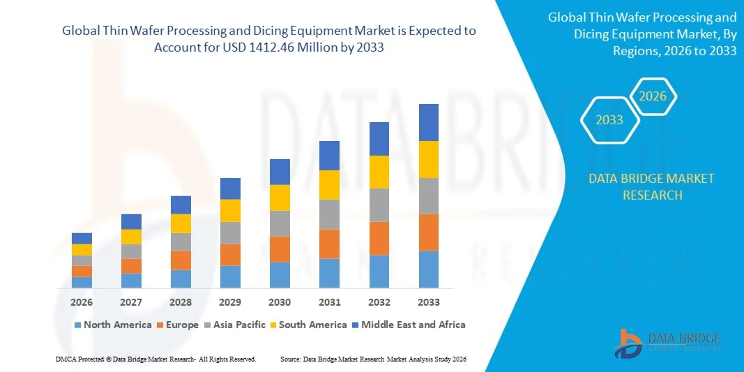
- The global thin wafer processing and dicing equipment market size was valued at USD 831.34 million in 2025 and is expected to reach USD 1412.46 million by 2033, at a CAGR of 6.85% during the forecast period
- Increasing demand for compact, high-performance, and power-efficient semiconductor devices, rising adoption of advanced packaging technologies such as TSV and 3D ICs, growing production of MEMS sensors, CMOS image sensors, and power devices, expansion of 5G infrastructure, electric vehicles, and IoT ecosystems, along with continuous innovation in laser and plasma dicing technologies are some of the major as well as vital factors which will such asly augment the growth of the thin wafer processing and dicing equipment market
What are the Major Takeaways of Thin Wafer Processing and Dicing Equipment Market?
- Growing demand for miniaturized consumer electronics, automotive semiconductors, and advanced memory and logic chips across emerging economies, along with increasing investments in semiconductor fabrication plants and R&D facilities, will further contribute by generating significant growth opportunities for the Thin Wafer Processing and Dicing Equipment market
- High capital investment requirements, technical complexities in ultra-thin wafer handling, yield loss risks during dicing processes, and shortage of skilled professionals are such asly to act as market restraint factors for the growth of the Thin Wafer Processing and Dicing Equipment market
- North America dominated the thin wafer processing and dicing equipment market with a highest revenue share of 41.36% in 2025, supported by strong semiconductor fabrication capacity, advanced packaging technologies, and rapid expansion of power electronics, MEMS, and compound semiconductor production across the U.S. and Canada
- Asia-Pacific is projected to register the fastest CAGR of 8.36% from 2026 to 2033, driven by large-scale semiconductor manufacturing, strong electronics export industries, and rapid expansion of advanced packaging facilities across China, Japan, South Korea, Taiwan, and India
- The Dicing Equipment segment dominated the market with a 41.6% share in 2025, driven by rising demand for precision wafer singulation in advanced semiconductor packaging
Report Scope and Thin Wafer Processing and Dicing Equipment Market Segmentation
|
Attributes |
Thin Wafer Processing and Dicing Equipment Key Market Insights |
|
Segments Covered |
|
|
Countries Covered |
North America
Europe
Asia-Pacific
Middle East and Africa
South America
|
|
Key Market Players |
|
|
Market Opportunities |
|
|
Value Added Data Infosets |
In addition to the insights on market scenarios such as market value, growth rate, segmentation, geographical coverage, and major players, the market reports curated by the Data Bridge Market Research also include in-depth expert analysis, pricing analysis, brand share analysis, consumer survey, demography analysis, supply chain analysis, value chain analysis, raw material/consumables overview, vendor selection criteria, PESTLE Analysis, Porter Analysis, and regulatory framework. |
What is the Key Trend in the Thin Wafer Processing and Dicing Equipment Market?
Increasing Adoption of Laser-Based, Ultra-Precision, and Automation-Integrated Dicing Technologies
- The thin wafer processing and dicing equipment market is witnessing strong adoption of advanced laser dicing, stealth dicing, and plasma dicing technologies designed to support ultra-thin wafers and high-density semiconductor architectures
- Manufacturers are introducing high-speed, automated systems with AI-enabled process control, real-time inspection, and precision alignment capabilities to improve yield and minimize wafer breakage
- Growing demand for compact, energy-efficient, and high-performance semiconductor devices is accelerating the shift toward ultra-thin wafer handling and advanced thinning solutions
- For instance, companies such as DISCO Corporation, ASMPT, EV Group, and Lam Research are expanding their portfolios with next-generation dicing and wafer thinning systems featuring improved accuracy and reduced kerf loss
- Increasing integration of temporary bonding/debonding systems and automated handling equipment is enhancing process reliability and throughput
- As semiconductor devices become thinner and more complex, thin wafer processing and dicing equipment will remain critical for advanced packaging, 3D IC integration, and high-yield chip manufacturing
What are the Key Drivers of Thin Wafer Processing And Dicing Equipment Market?
- Rising demand for miniaturized, lightweight, and high-performance semiconductor devices across consumer electronics, automotive, telecommunications, and industrial applications
- For instance, in 2025, leading semiconductor equipment manufacturers expanded investments in laser dicing, plasma thinning, and precision wafer handling technologies to support advanced node production
- Growing adoption of 5G devices, AI processors, electric vehicles, MEMS sensors, and CMOS image sensors is boosting demand for ultra-thin wafer processing solutions across Asia-Pacific, North America, and Europe
- Advancements in temporary bonding technologies, precision grinding, and automated inspection systems have improved production efficiency and reduced wafer damage risks
- Increasing establishment of new semiconductor fabrication facilities and packaging plants is creating sustained demand for high-precision dicing and thinning equipment
- Supported by continuous innovation in semiconductor manufacturing and strong global investments in chip production capacity, the thin wafer processing and dicing equipment market is expected to witness steady long-term growth
Which Factor is Challenging the Growth of the Thin Wafer Processing And Dicing Equipment Market?
- High capital investment requirements associated with advanced laser dicing systems, plasma equipment, and automated wafer handling solutions limit adoption among small and mid-scale semiconductor manufacturers
- For instance, during 2024–2025, fluctuations in raw material prices, supply chain disruptions, and component shortages increased equipment manufacturing and procurement costs
- Technical challenges in handling ultra-thin wafers, including breakage risks, warpage, and yield loss, increase operational complexity
- Requirement for highly skilled engineers and specialized process expertise raises operational expenses
- Competition from alternative packaging technologies and process optimization strategies may impact equipment replacement cycles
- To address these challenges, companies are focusing on cost-efficient system designs, enhanced automation, predictive maintenance solutions, and improved training programs to increase global adoption of thin wafer processing and dicing equipment
How is the Thin Wafer Processing and Dicing Equipment Market Segmented?
The market is segmented on the basis of channel count, application, and vertical.
- By Equipment Type
On the basis of equipment type, the thin wafer processing and dicing equipment market is segmented into Thinning Equipment, Dicing Equipment, and Handling & Support Equipment. The Dicing Equipment segment dominated the market with a 41.6% share in 2025, driven by rising demand for precision wafer singulation in advanced semiconductor packaging. Technologies such as blade dicing, laser dicing, and plasma dicing are widely adopted to ensure minimal kerf loss and higher chip yield. Increasing production of MEMS devices, power semiconductors, and CMOS image sensors further supports demand.
The Handling & Support Equipment segment is expected to grow at the fastest CAGR from 2026 to 2033, supported by increasing adoption of temporary bonding/debonding systems and automated wafer handling solutions required for ultra-thin wafer processing and high-volume manufacturing environments.
- By Wafer Size
On the basis of wafer size, the market is segmented into Less than 4 inch, 5 inch and 6 inch, 8 inch, and 12 inch. The 12 inch segment dominated the market with a 45.3% share in 2025, as 300 mm wafers are widely used in advanced semiconductor fabrication for logic, memory, and high-performance computing devices. Larger wafer sizes enable higher chip output per wafer, improving manufacturing efficiency and cost optimization.
The 8 inch segment is projected to grow at the fastest CAGR from 2026 to 2033, driven by strong demand for power devices, MEMS sensors, and automotive semiconductors, where mature node production continues to expand globally.
- By Wafer Thickness
On the basis of wafer thickness, the market is segmented into 750 µm standard or less thin, 120 µm advanced mainstream, and 50 µm and below. The 120 µm advanced mainstream segment dominated the market with a 38.9% share in 2025, supported by its widespread use in advanced packaging, 3D IC integration, and mobile device components. This thickness range offers a balance between mechanical stability and device miniaturization.
The 50 µm and below segment is expected to grow at the fastest CAGR from 2026 to 2033, driven by increasing demand for ultra-thin chips in wearables, IoT devices, and high-density stacked semiconductor architectures.
- By Application
On the basis of application, the market is segmented into CMOS image sensors, Memory and logic TSV, MEMS device, Power device, RFID, and Others. The Memory and logic TSV segment dominated the market with a 40.2% share in 2025, driven by rapid expansion of high-performance computing, AI processors, and advanced 3D packaging technologies. TSV integration requires precise wafer thinning and dicing to ensure reliability and performance.
The Power device segment is projected to grow at the fastest CAGR from 2026 to 2033, supported by increasing adoption of electric vehicles, renewable energy systems, and industrial power management solutions.
- By End Use Industry
On the basis of end use industry, the thin wafer processing and dicing equipment market is segmented into Consumer electronics, Automotive, Telecommunications, Healthcare, Aerospace & Defense, Industrial, and Others. The Consumer electronics segment dominated the market with a 37.5% share in 2025, driven by high production volumes of smartphones, tablets, laptops, and wearable devices requiring advanced semiconductor components.
The Automotive segment is expected to grow at the fastest CAGR from 2026 to 2033, propelled by rising adoption of EVs, ADAS systems, power electronics, and vehicle connectivity technologies that require high-reliability semiconductor devices.
Which Region Holds the Largest Share of the Thin Wafer Processing and Dicing Equipment Market?
- North America dominated the thin wafer processing and dicing equipment market with a highest revenue share of 41.36% in 2025, supported by strong semiconductor fabrication capacity, advanced packaging technologies, and rapid expansion of power electronics, MEMS, and compound semiconductor production across the U.S. and Canada. High demand for ultra-thin wafers in 3D ICs, AI processors, automotive chips, and advanced memory devices continues to drive adoption of precision grinding, polishing, and dicing systems across foundries, IDMs, and OSAT facilities
- Leading equipment manufacturers in North America are introducing high-precision, automated, and AI-enabled wafer thinning and dicing solutions featuring real-time monitoring, laser-based dicing, and advanced stress-control mechanisms, strengthening the region’s technological leadership. Continuous investments in advanced semiconductor nodes, heterogeneous integration, and wafer-level packaging further support long-term expansion
- Strong R&D infrastructure, presence of major semiconductor companies, and sustained capital expenditure in fabrication plants reinforce regional dominance in thin wafer processing technologies
U.S. Thin Wafer Processing and Dicing Equipment Market Insight
The U.S. is the largest contributor in North America, driven by substantial investments in semiconductor manufacturing, advanced node development, and domestic chip production initiatives. Rising production of AI accelerators, high-performance computing chips, automotive semiconductors, and defense electronics increases demand for ultra-precise wafer thinning and stealth dicing equipment. Expansion of wafer-level packaging, chiplet integration, and 3D stacking technologies further strengthens market growth across leading fabs and research facilities.
Canada Thin Wafer Processing and Dicing Equipment Market Insight
Canada supports regional growth through expanding semiconductor research programs, growing MEMS and photonics development, and increasing collaboration between universities and fabrication facilities. Demand for thin wafer processing tools is rising in power electronics, aerospace components, and telecom infrastructure applications. Government-backed innovation initiatives and skilled engineering talent contribute to steady adoption of advanced wafer handling and precision dicing systems.
Asia-Pacific Thin Wafer Processing and Dicing Equipment Market
Asia-Pacific is projected to register the fastest CAGR of 8.36% from 2026 to 2033, driven by large-scale semiconductor manufacturing, strong electronics export industries, and rapid expansion of advanced packaging facilities across China, Japan, South Korea, Taiwan, and India. High-volume production of memory chips, logic ICs, power devices, and consumer electronics significantly increases demand for high-throughput wafer grinding and dicing equipment. Growth in EV electronics, 5G infrastructure, AI chips, and industrial automation further accelerates adoption of advanced thin wafer technologies across the region.
China Thin Wafer Processing and Dicing Equipment Market Insight
China is a major contributor to Asia-Pacific growth due to extensive semiconductor investments, expanding domestic fabrication capacity, and strong government support for chip self-sufficiency. Rising development of advanced nodes, power semiconductors, and compound semiconductor devices increases demand for precision wafer thinning and laser dicing solutions. Competitive manufacturing ecosystems and large-scale production volumes enhance regional equipment deployment.
Japan Thin Wafer Processing and Dicing Equipment Market Insight
Japan demonstrates steady growth supported by its strong presence in semiconductor equipment manufacturing, precision engineering, and advanced materials. High adoption of ultra-thin wafer technologies in automotive electronics, image sensors, and industrial robotics drives demand for high-accuracy grinding and dicing systems. Continuous innovation in wafer handling automation and defect reduction technologies supports long-term expansion.
India Thin Wafer Processing and Dicing Equipment Market Insight
India is emerging as a promising growth market due to increasing semiconductor design activities, government-backed fabrication initiatives, and expanding electronics manufacturing clusters. Rising focus on domestic chip production, automotive electronics, and telecom hardware fuels demand for wafer processing and dicing solutions in pilot production and R&D facilities. Strengthening semiconductor ecosystem development further enhances future market penetration.
South Korea Thin Wafer Processing and Dicing Equipment Market Insight
South Korea contributes significantly to regional growth due to its global leadership in memory chips, advanced logic devices, and display technologies. Growing production of high-density DRAM, NAND, and AI processors increases demand for ultra-thin wafer grinding and high-precision dicing equipment. Strong manufacturing infrastructure, continuous technology upgrades, and heavy R&D investment sustain long-term market growth.
Which are the Top Companies in Thin Wafer Processing and Dicing Equipment Market?
The thin wafer processing and dicing equipment industry is primarily led by well-established companies, including:
- Advanced Dicing Technologies (Israel)
- ASMPT (Singapore)
- AXUS TECHNOLOGY (U.S.)
- Citizen Chiba Precision Co., Ltd. (Japan)
- DISCO Corporation (Japan)
- Dynatex International (U.S.)
- EV Group (EVG) (Austria)
- HANMI Semiconductor (South Korea)
- Han's Laser Technology Co., Ltd. (China)
- KLA Corporation (U.S.)
- Lam Research Corporation (U.S.)
What are the Recent Developments in Global Thin Wafer Processing and Dicing Equipment Market?
- In September 2025, Panasonic Industry committed JPY 17 billion (USD 115 million) to establish a new manufacturing facility in Thailand focused on producing multilayer circuit-board materials for AI server modules, strengthening its position in advanced electronics materials and supporting the growing demand for high-performance semiconductor packaging applications, thereby reinforcing supply chain capabilities in Asia
- In April 2025, Tokyo Electron and IBM renewed their five-year research and development partnership to advance laser debonding and plasma dicing technologies tailored for sub-2 nm semiconductor nodes, aiming to improve precision and yield in next-generation wafer processing, thereby accelerating innovation in advanced chip manufacturing processes
- In April 2025, China accelerated its strategy to consolidate nearly 200 domestic semiconductor equipment manufacturers into 10 larger groups to enhance indigenous production capacity and technological competitiveness, strengthening the country’s self-reliance in chip-tool development, thereby boosting domestic equipment capabilities in the thin wafer processing ecosystem
- In February 2025, 3M joined the US-JOINT Consortium to collaboratively develop next-generation advanced packaging materials at a newly established Silicon Valley R&D hub, supporting innovation in wafer-level and heterogeneous integration technologies, thereby enhancing material advancements for thin wafer processing and dicing applications
- In December 2022, DISCO Corporation introduced the DFG8541, a fully automated grinding system capable of processing silicon and silicon carbide wafers up to 8 inches in diameter, improving efficiency and precision in wafer thinning operations, thereby strengthening high-performance semiconductor manufacturing capabilities.
- In January 2021, UTAC Holdings Ltd. completed the acquisition of Singapore-based wafer bumping assets from Powertech Technology (Singapore) Pte. Ltd., and entered into Transitional Services and License Agreements to ensure seamless operational transfer, thereby expanding its advanced packaging and wafer-level service portfolio
SKU-
- Interactive Data Analysis Dashboard
- Company Analysis Dashboard for high growth potential opportunities
- Research Analyst Access for customization & queries
- Competitor Analysis with Interactive dashboard
- Latest News, Updates & Trend analysis
- Harness the Power of Benchmark Analysis for Comprehensive Competitor Tracking
Global Thin Wafer Processing And Dicing Equipment Market, Supply Chain Analysis and Ecosystem Framework
To support market growth and help clients navigate the impact of geopolitical shifts, DBMR has integrated in-depth supply chain analysis into its Global Thin Wafer Processing And Dicing Equipment Market research reports. This addition empowers clients to respond effectively to global changes affecting their industries. The supply chain analysis section includes detailed insights such as Global Thin Wafer Processing And Dicing Equipment Market consumption and production by country, price trend analysis, the impact of tariffs and geopolitical developments, and import and export trends by country and HSN code. It also highlights major suppliers with data on production capacity and company profiles, as well as key importers and exporters. In addition to research, DBMR offers specialized supply chain consulting services backed by over a decade of experience, providing solutions like supplier discovery, supplier risk assessment, price trend analysis, impact evaluation of inflation and trade route changes, and comprehensive market trend analysis.
Data collection and base year analysis are done using data collection modules with large sample sizes. The stage includes obtaining market information or related data through various sources and strategies. It includes examining and planning all the data acquired from the past in advance. It likewise envelops the examination of information inconsistencies seen across different information sources. The market data is analysed and estimated using market statistical and coherent models. Also, market share analysis and key trend analysis are the major success factors in the market report. To know more, please request an analyst call or drop down your inquiry.
The key research methodology used by DBMR research team is data triangulation which involves data mining, analysis of the impact of data variables on the market and primary (industry expert) validation. Data models include Vendor Positioning Grid, Market Time Line Analysis, Market Overview and Guide, Company Positioning Grid, Patent Analysis, Pricing Analysis, Company Market Share Analysis, Standards of Measurement, Global versus Regional and Vendor Share Analysis. To know more about the research methodology, drop in an inquiry to speak to our industry experts.
Data Bridge Market Research is a leader in advanced formative research. We take pride in servicing our existing and new customers with data and analysis that match and suits their goal. The report can be customized to include price trend analysis of target brands understanding the market for additional countries (ask for the list of countries), clinical trial results data, literature review, refurbished market and product base analysis. Market analysis of target competitors can be analyzed from technology-based analysis to market portfolio strategies. We can add as many competitors that you require data about in the format and data style you are looking for. Our team of analysts can also provide you data in crude raw excel files pivot tables (Fact book) or can assist you in creating presentations from the data sets available in the report.


