

What is the Vapor Deposition Market Size and Growth Rate?
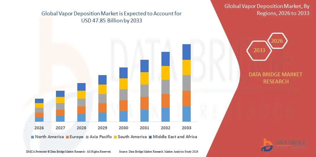
- As per Data Bridge Market Research analysis, the vapor deposition market was valued at USD 24.68 billion in 2025 and is projected to reach USD 47.85 billion by 2033, growing at a CAGR of 8.65% from 2026 to 2033.
- The market is experiencing strong growth driven by escalating demand for advanced semiconductor nodes, rising investment in wafer fabrication capacity, and the rapid expansion of solar photovoltaic and optical coating applications worldwide.
- The accelerating shift toward miniaturized, high-performance electronic devices, combined with government-backed semiconductor self-sufficiency initiatives across the U.S., Europe, and Asia-Pacific, is compelling foundries, research institutions, and industrial coating providers to expand deposition capacity. PVD and ALD systems are increasingly replacing conventional coating methods, offering superior film uniformity, atomic-level thickness control, and improved yield for next-generation chip architectures.
Market Size & Forecast
- Global Market Value (2025): USD 24.68 Billion
- Expected Market Value (2033): USD 47.85 Billion
- Forecast CAGR (2026–2033): 8.65%
- Leading Region in 2025: Asia-Pacific
- Fastest Growing Region: North America
What are the Major Takeaways of the Vapor Deposition Market?
- Asia-Pacific dominated the global vapor deposition market with the largest revenue share of 38.72% in 2025, supported by dense semiconductor fabrication capacity, large-scale solar panel manufacturing, and strong government investment across China, South Korea, Taiwan, and Japan.
- North America is expected to be the fastest-growing region at a CAGR of 10.1% from 2026 to 2033, fueled by CHIPS Act-driven fab expansion, reshoring of advanced semiconductor manufacturing, and growing investment in domestic equipment supply chains.
- The physical vapor deposition (PVD) segment led the market with a 34.85% share in 2025, driven by its widespread use in metallization, hard coatings, and decorative finishing across semiconductor and industrial applications.
- Atomic layer deposition (ALD) is the fastest-growing technology segment, projected to register a CAGR of 11.2%, reflecting rising demand for ultra-thin, conformal films in advanced logic and memory devices.
- The semiconductor & integrated circuits segment dominated the application category with a 41.20% revenue share in 2025, led by escalating demand for AI accelerators, advanced logic nodes, and high-bandwidth memory.
- The semiconductor foundries & IDMs segment is the fastest-growing end-user category, with a CAGR of 9.6%, driven by aggressive capacity expansion among leading-edge chipmakers.
Report Scope and Vapor Deposition Market Segmentation
|
Attributes |
Vapor Deposition Key Market Insights |
|
Segments Covered |
|
|
Countries Covered |
North America
Europe
Asia-Pacific
Middle East and Africa
South America
|
|
Key Market Players |
|
|
Market Opportunities |
Market Opportunities
|
|
Value Added Data Infosets |
Value Added Data Infosets In addition to the insights on market scenarios such as market value, growth rate, segmentation, geographical coverage, and major players, the market reports curated by the Data Bridge Market Research also include in-depth expert analysis, geographically represented company-wise production and capacity, network layouts of distributors and partners, detailed and updated price trend analysis, and deficit analysis of supply chain and demand. |
What is the Key Trend in the Vapor Deposition Market?
- Semiconductor manufacturers are increasingly adopting atomic layer deposition and advanced PVD platforms to enable sub-3nm node production, driven by the need for atomic-scale precision, uniform step coverage, and defect-free thin films in transistor and interconnect fabrication.
- For instance, in March 2025, Applied Materials introduced an enhanced ALD platform incorporating AI-based process control, enabling real-time film thickness correction and improved yield for gate-all-around (GAA) transistor architectures used in next-generation logic chips.
- In-situ metrology and machine-learning-driven predictive maintenance are enabling equipment makers to reduce unplanned downtime and improve first-pass yield across high-volume fabs.
- Coating providers are leveraging vapor deposition to deliver ultra-durable, low-friction, and corrosion-resistant surfaces for cutting tools, aerospace components, and medical implants, expanding the technology's footprint beyond electronics.
- For instance, in February 2025, Oerlikon Balzers expanded its PVD coating service network in North America to support growing demand for wear-resistant tooling coatings from the automotive and aerospace machining sectors.
- As chipmakers and industrial manufacturers continue to prioritize film precision, throughput, and sustainability, the adoption of advanced vapor deposition technologies is expected to accelerate, reinforcing deposition as a foundational process in semiconductor and advanced materials manufacturing.
What are the Key Drivers of the Vapor Deposition Market?
- The rapid advancement of AI accelerators, high-bandwidth memory, and advanced logic nodes has significantly increased demand for high-precision deposition equipment capable of depositing atomically thin, uniform films across increasingly complex 3D chip structures.
- For instance, in March 2025, Lam Research expanded its portfolio of selective deposition systems designed to support gate-all-around transistor manufacturing and advanced packaging applications for AI and high-performance computing chips.
- Government-backed semiconductor manufacturing initiatives, including the U.S. CHIPS Act, the EU Chips Act, and similar programs across Japan, South Korea, and India, are driving substantial capital investment in new fabrication facilities, directly boosting demand for deposition tools.
- For instance, in November 2024, ASM International announced capacity expansion at its ALD manufacturing facility in South Korea to meet rising orders from regional memory and foundry customers investing in advanced node capacity.
- With the semiconductor and renewable energy industries increasingly reliant on precise, scalable thin-film deposition to accelerate innovation and improve device performance, vapor deposition technologies will remain indispensable for next-generation electronics, solar, and industrial coating applications.
Which Factors are Challenging the Growth of the Vapor Deposition Market?
- Advanced vapor deposition systems require substantial upfront capital investment due to the integration of high-vacuum chambers, precision plasma sources, automated wafer-handling robotics, and in-situ process monitoring systems.
- These high costs limit adoption among smaller coating job shops, research laboratories, and manufacturers in emerging economies, slowing broader market penetration.
- For instance, in October 2024, a leading European research consortium highlighted that installation of a fully automated high-volume ALD cluster tool can require capital outlays well in excess of several million dollars, underscoring the substantial financial commitment required to deploy next-generation deposition infrastructure.
- The high capital investment, coupled with recurring costs for high-purity precursor gases, target materials, and specialized maintenance, continues to restrict adoption among small and medium-sized enterprises. This cost barrier slows market penetration in price-sensitive and emerging regions, limiting the widespread deployment of advanced deposition technologies despite growing underlying demand.
How is the Vapor Deposition Market Segmented?
The vapor deposition market is segmented on the basis of technology, application, and end user.
- By Technology
On the basis of technology, the global vapor deposition market is segmented into physical vapor deposition (PVD), chemical vapor deposition (CVD), atomic layer deposition (ALD), plasma-enhanced chemical vapor deposition (PECVD), and metal-organic chemical vapor deposition (MOCVD). The physical vapor deposition segment dominated the market with a 34.85% share in 2025, owing to its widespread use in metallization, decorative finishing, and hard-coating applications across semiconductor, tooling, and consumer electronics manufacturing. These systems deliver strong adhesion and film uniformity without the need for reactive precursor chemistries, making them the preferred choice for high-volume production environments.
The atomic layer deposition segment is projected to register the fastest growth at a CAGR of 11.2% from 2026 to 2033, driven by rising demand for ultra-thin, conformal, and pinhole-free films in advanced logic, memory, and gate-all-around transistor manufacturing. Increasing adoption in emerging applications such as flexible electronics and next-generation battery materials is further accelerating segment expansion.
- By Application
On the basis of application, the global vapor deposition market is segmented into semiconductor & integrated circuits, solar & photovoltaic cells, optical coatings, cutting tools & industrial coatings, data storage devices, medical devices, and decorative & packaging coatings. The semiconductor & integrated circuits segment dominated the market with a share of 41.20% in 2025 due to its widespread adoption by leading-edge foundries and IDMs, increasing demand for AI and high-performance computing chips, and growing integration of advanced thin-film technologies such as ALD and selective deposition. additionally, rising focus on transistor miniaturization, interconnect reliability, and advanced packaging further supports the strong adoption of vapor deposition solutions.
The solar & photovoltaic cells segment is anticipated to witness the fastest CAGR of 9.8% from 2026 to 2033, driven by the increasing global buildout of thin-film and high-efficiency solar cell manufacturing capacity. Solar manufacturers are adopting advanced CVD and PECVD platforms to improve cell efficiency, reduce material consumption, and support scalable, cost-effective production. additionally, the integration of automated inline deposition systems is enhancing throughput and process consistency, further driving segment growth.
- By End User
On the basis of end user, the global vapor deposition market is segmented into semiconductor foundries & IDMs, aerospace & defense, automotive, healthcare & medical device manufacturers, energy & solar, consumer electronics, and tool & die manufacturers. The semiconductor foundries & IDMs segment dominated the market with a share of 36.05% in 2025 due to its critical role in advanced node fabrication, memory production, and advanced packaging. the widespread adoption of high-precision ALD, PVD, and CVD platforms for gate stack formation, interconnect metallization, and barrier layer deposition is driving strong demand for deposition solutions. additionally, increasing capital expenditure on new fab construction and capacity expansion is reinforcing the dominance of this segment across global markets.
The semiconductor foundries & IDMs segment is also expected to witness the fastest CAGR of 9.6% from 2026 to 2033, driven by the rising need for advanced logic and memory manufacturing capacity. Foundries are increasingly integrating next-generation deposition tools into leading-edge process nodes to reduce defect density and improve device performance. additionally, the growing emphasis on domestic chip manufacturing and supply chain resilience is further accelerating the adoption of deposition technologies across foundries and IDMs.
Which Region Holds the Largest Share of the Vapor Deposition Market?
- Asia-Pacific dominated the vapor deposition market and accounted for the largest revenue share of 38.72% in 2025, supported by dense semiconductor fabrication capacity, large-scale solar manufacturing, and the presence of leading foundries and equipment integrators across China, South Korea, Taiwan, and Japan.
- The region also benefits from aggressive government-backed capital investment in fab construction, a well-established electronics supply chain, and growing adoption of advanced ALD and PVD platforms for leading-edge logic and memory production. Continued expansion of advanced packaging and renewable energy manufacturing continues to strengthen Asia-Pacific's leadership position in the global market.
China Vapor Deposition Market Insight
The China vapor deposition market is expanding rapidly, supported by large-scale investment in domestic semiconductor manufacturing, growing memory and foundry capacity, and government initiatives aimed at strengthening chip supply chain self-sufficiency. Increasing adoption of PVD, CVD, and ALD platforms across both semiconductor and solar panel manufacturing is contributing to sustained market growth. Furthermore, rising investment by domestic equipment makers in indigenous deposition technologies is positioning China as a key growth engine for the global vapor deposition industry.
South Korea Vapor Deposition Market Insight
The South Korea vapor deposition market is witnessing steady growth, driven by the country's dominant position in global memory chip manufacturing and continued capacity expansion by leading foundries. Automotive and display manufacturers are also increasingly utilizing deposition technologies for advanced coatings and thin-film applications. Continuous advancements in ALD process technology, along with strong government focus on semiconductor competitiveness, are further reinforcing market growth in South Korea.
North America Vapor Deposition Market Insight
The North America vapor deposition market is expected to witness the fastest growth globally, driven by CHIPS Act-backed fab construction, reshoring of advanced semiconductor manufacturing, and rising investment in domestic equipment and materials supply chains. Growing demand for AI accelerators, advanced packaging, and next-generation power electronics is supporting regional market expansion. Additionally, the growing presence of leading equipment makers and research institutions is accelerating deposition technology adoption across commercial and academic sectors.
U.S. Vapor Deposition Market Insight
The U.S. vapor deposition market is experiencing robust growth, supported by rising investment in leading-edge fab construction, expanding demand for AI and high-performance computing chips, and growing federal funding for domestic semiconductor manufacturing. Increasing collaboration between equipment makers, foundries, and research institutions is improving deposition process performance and accelerating technology adoption. Furthermore, integration of AI-driven process control and predictive maintenance technologies is improving equipment uptime and positioning the U.S. as a key innovation hub in the vapor deposition industry.
Germany Vapor Deposition Market Insight
The Germany vapor deposition market is expanding steadily due to the country's strong industrial coatings base, advanced research capabilities, and growing semiconductor equipment manufacturing footprint. Automotive, tooling, and optics companies are increasingly utilizing deposition technologies for wear-resistant and precision optical coatings. Continuous advancements in sputtering and evaporation technologies, along with strong government focus on advanced manufacturing, are further driving market growth in Germany.
Which are the Top Companies in Vapor Deposition Market?
The vapor deposition industry is primarily led by well-established companies, including:
- Applied Materials, Inc. (U.S.)
- Lam Research Corporation (U.S.)
- ASM International N.V. (Netherlands)
- Veeco Instruments Inc. (U.S.)
- Tokyo Electron Limited (Japan)
- ULVAC, Inc. (Japan)
- AIXTRON SE (Germany)
- Oerlikon Balzers (Liechtenstein)
- Kurt J. Lesker Company (U.S.)
- Denton Vacuum, LLC (U.S.)
- Bühler Leybold Optics (Germany)
- CVD Equipment Corporation (U.S.)
- Beneq Oy (Finland)
- Hitachi High-Tech Corporation (Japan)
- Plasma-Therm LLC (U.S.)
What are Latest Developments in Vapor Deposition Market?
- In September 2025, Applied Materials unveiled its next-generation Endura ALD platform, featuring AI-enabled process control and improved wafer throughput, setting a new benchmark for atomic-scale deposition across advanced logic, memory, and packaging applications. The upgraded platform delivers enhanced film uniformity, reduced defectivity, and improved uptime, reflecting continued innovation in high-volume manufacturing deposition tools. This launch strengthens Applied Materials' market leadership by boosting process precision, throughput, and yield for leading-edge chipmakers.
- In January 2025, Lam Research completed the acquisition of a specialized dry-etch and deposition technology provider, strengthening its technological and industrial capabilities in advanced patterning and thin-film integration. The deal integrates complementary process expertise with Lam's existing deposition platforms, broadening its product offerings for gate-all-around transistor and advanced packaging applications. This strategic acquisition accelerates Lam Research's innovation in advanced node technologies, creating synergies that expand its reach across leading foundry and memory customers.
- In November 2025, ASM International launched a new generation of its ALD system for selective deposition, the latest addition to its process portfolio used for advanced logic and memory device fabrication. The new release improves deposition selectivity by integrating enhanced precursor delivery and chamber design, allowing chipmakers to reduce process steps at advanced nodes. It also includes improved in-situ metrology and expanded compatibility with high-mobility channel materials. This development strengthens ASM International's position in the vapor deposition market, as the new system enables customers to achieve tighter process control in a smaller equipment footprint.
- In November 2024, Aixtron SE released an upgraded MOCVD platform, introducing new reactor design capabilities including improved temperature uniformity and higher wafer capacity per run. The update allows compound semiconductor manufacturers to produce GaN and SiC-based power devices more efficiently. These features help power electronics and RF device makers improve yield and reduce production costs, while the upgrade also expanded platform compatibility for micro-LED display manufacturing.
- In June 2023, Veeco Instruments participated in a multi-partner research initiative, collaborating with research institutes and industry partners to advance next-generation laser-assisted deposition technologies. The company contributed its ALD and MOCVD platforms to support process development for compound semiconductor and photonics applications in joint pilot-line programs. This collaboration demonstrates the application of vapor deposition technologies in research and development of advanced materials and next-generation device architectures.
- Interactive Data Analysis Dashboard
- Company Analysis Dashboard for high growth potential opportunities
- Research Analyst Access for customization & queries
- Competitor Analysis with Interactive dashboard
- Latest News, Updates & Trend analysis
- Harness the Power of Benchmark Analysis for Comprehensive Competitor Tracking
Global Vapor Deposition Market, Supply Chain Analysis and Ecosystem Framework
To support market growth and help clients navigate the impact of geopolitical shifts, DBMR has integrated in-depth supply chain analysis into its Global Vapor Deposition Market research reports. This addition empowers clients to respond effectively to global changes affecting their industries. The supply chain analysis section includes detailed insights such as Global Vapor Deposition Market consumption and production by country, price trend analysis, the impact of tariffs and geopolitical developments, and import and export trends by country and HSN code. It also highlights major suppliers with data on production capacity and company profiles, as well as key importers and exporters. In addition to research, DBMR offers specialized supply chain consulting services backed by over a decade of experience, providing solutions like supplier discovery, supplier risk assessment, price trend analysis, impact evaluation of inflation and trade route changes, and comprehensive market trend analysis.
Data collection and base year analysis are done using data collection modules with large sample sizes. The stage includes obtaining market information or related data through various sources and strategies. It includes examining and planning all the data acquired from the past in advance. It likewise envelops the examination of information inconsistencies seen across different information sources. The market data is analysed and estimated using market statistical and coherent models. Also, market share analysis and key trend analysis are the major success factors in the market report. To know more, please request an analyst call or drop down your inquiry.
The key research methodology used by DBMR research team is data triangulation which involves data mining, analysis of the impact of data variables on the market and primary (industry expert) validation. Data models include Vendor Positioning Grid, Market Time Line Analysis, Market Overview and Guide, Company Positioning Grid, Patent Analysis, Pricing Analysis, Company Market Share Analysis, Standards of Measurement, Global versus Regional and Vendor Share Analysis. To know more about the research methodology, drop in an inquiry to speak to our industry experts.
Data Bridge Market Research is a leader in advanced formative research. We take pride in servicing our existing and new customers with data and analysis that match and suits their goal. The report can be customized to include price trend analysis of target brands understanding the market for additional countries (ask for the list of countries), clinical trial results data, literature review, refurbished market and product base analysis. Market analysis of target competitors can be analyzed from technology-based analysis to market portfolio strategies. We can add as many competitors that you require data about in the format and data style you are looking for. Our team of analysts can also provide you data in crude raw excel files pivot tables (Fact book) or can assist you in creating presentations from the data sets available in the report.