
Global Wafer Fabrication Equipment Market
Market Size in USD Billion
 USD
89.64 Billion
USD
152.78 Billion
2025
2033
USD
89.64 Billion
USD
152.78 Billion
2025
2033
| 2026 - 2033 | |
| USD 89.64 Billion | |
| USD 152.78 Billion | |
| % | |
|
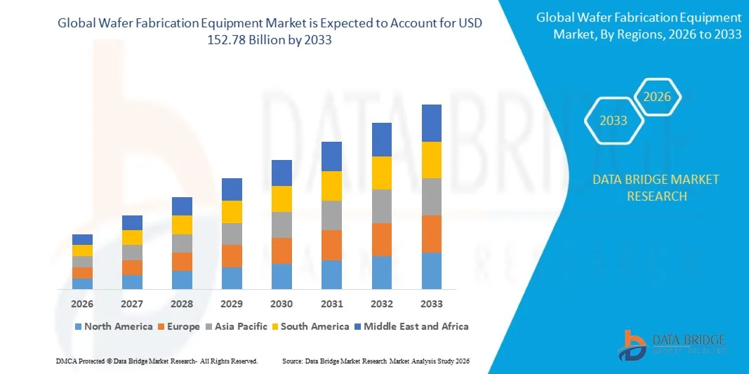
Wafer Fabrication Equipment Market Size
- The Wafer Fabrication Equipment Market size was valued at USD 89.64 billion in 2025 and is expected to reach USD 152.78billion by 2033, at a CAGR of 6.9% during the forecast period
- The market growth is primarily driven by the increasing demand for advanced semiconductor devices, rising investments in semiconductor manufacturing facilities, and growing adoption of high-performance computing, artificial intelligence, and 5G technologies across industries.
- Additionally, increasing investments in next-generation semiconductor fabrication technologies, rapid expansion of consumer electronics production, growing adoption of electric vehicles, and continuous advancements in wafer processing and lithography technologies are significantly contributing to sustained market expansion.
Global Wafer Fabrication Equipment Market Analysis
- Wafer Fabrication Equipment refers to specialized semiconductor manufacturing systems and process equipment used for the fabrication of integrated circuits and semiconductor wafers, including deposition, lithography, etching, cleaning, ion implantation, and inspection processes across semiconductor production facilities.
- The increasing demand for Wafer Fabrication Equipment is driven by the growing deployment of advanced semiconductor chips, rising investments in semiconductor foundries, increasing need for smaller and more efficient chip architectures, and expanding utilization of semiconductors across industries such as consumer electronics, automotive, telecommunications, industrial automation, and healthcare.
- North America dominated the wafer fabrication equipment market with the 43.56% revenue share in 2025, supported by strong presence of leading semiconductor technology providers, high investments in semiconductor research and development, advanced chip manufacturing infrastructure, and increasing adoption of AI and high-performance computing technologies.
- Asia-Pacific is expected to witness the 7.2% growth during the forecast period due to rising semiconductor manufacturing investments, increasing government support for domestic chip production, expanding consumer electronics industry, and growing adoption of advanced semiconductor technologies in countries such as China, Taiwan, South Korea, Japan, and India.
- The lithography equipment segment dominated the market with the 26.55% market share in 2025, driven by increasing demand for advanced semiconductor nodes, growing adoption of EUV lithography technologies, and rising investments in next-generation semiconductor manufacturing processes.
Report Scope and Wafer Fabrication Equipment Market Segmentation
|
Attributes |
GlobalWafer Fabrication Equipment Key Market Insights |
|
Segments Covered |
|
|
Countries Covered |
North America · U.S. · Canada · Mexico Europe · Germany · France · U.K. · Netherlands · Switzerland · Belgium · Russia · Italy · Spain · Turkey · Rest of Europe Asia-Pacific · China · Japan · India · South Korea · Singapore · Malaysia · Australia · Thailand · Indonesia · Philippines · Rest of Asia-Pacific Middle East and Africa · Saudi Arabia · U.A.E. · South Africa · Egypt · Israel · Rest of Middle East and Africa South America · Brazil · Argentina · Rest of South America |
|
Key Market Players |
· Applied Materials, Inc. (U.S.) · ASML Holding N.V. (Netherlands) · Tokyo Electron Limited (Japan) · Lam Research Corporation (U.S.) · KLA Corporation (U.S.) · SCREEN Holdings Co., Ltd. (Japan) · Hitachi High-Tech Corporation (Japan) · Canon Inc. (Japan) · Nikon Corporation (Japan) · ASM International N.V. (Netherlands) · Teradyne, Inc. (U.S.) · Advantest Corporation (Japan) |
|
Market Opportunities |
· Increasing demand for advanced semiconductor manufacturing technologies, rising adoption of AI chips, high-performance computing systems, and 5G-enabled devices along with growing investments in semiconductor fabrication facilities globally · Growth in adoption of EUV lithography systems, advanced wafer inspection technologies, next-generation deposition and etching equipment, and automated semiconductor manufacturing solutions for improving chip production efficiency and process precision |
|
Value Added Data Infosets |
In addition to the insights on market scenarios such as market value, growth rate, segmentation, geographical coverage, and major players, the market reports curated by the Data Bridge Market Research also include in-depth expert analysis, geographically represented company-wise production and capacity, network layouts of distributors and partners, detailed and updated price trend analysis and deficit analysis of supply chain and demand. |
Wafer Fabrication Equipment Market Trends
“Growing Adoption of Advanced Semiconductor Manufacturing and EUV Lithography Technologies”
- A significant and accelerating trend in the Wafer Fabrication Equipment Market is the increasing adoption of advanced semiconductor manufacturing technologies and extreme ultraviolet (EUV) lithography systems, driven by the growing demand for high-performance semiconductor chips, miniaturized electronic devices, and advanced computing applications.
- The adoption of advanced technologies such as EUV lithography, atomic layer deposition, advanced wafer inspection systems, AI-enabled semiconductor manufacturing analytics, and automated process control platforms is enabling semiconductor manufacturers to improve production efficiency, enhance chip precision, reduce defect rates, and accelerate next-generation semiconductor fabrication processes.
- Rising demand for integrated semiconductor manufacturing ecosystems is further driving market growth, as semiconductor companies increasingly prefer unified fabrication platforms that combine deposition, etching, inspection, metrology, and wafer processing technologies into centralized semiconductor production environments.
- Increasing focus on advanced chip architectures and smaller process nodes is encouraging the development of next-generation wafer fabrication equipment capable of supporting high-density semiconductor integration and enhanced manufacturing precision.
- The expansion of semiconductor manufacturing investments is boosting demand for Wafer Fabrication Equipment solutions, particularly in emerging semiconductor hubs such as China, Taiwan, South Korea, and India, where investments in domestic semiconductor production infrastructure are increasing significantly.
- Continuous innovation in semiconductor process technologies, AI-driven manufacturing automation, advanced lithography systems, and wafer inspection platforms, along with increasing focus on production scalability and process efficiency, is driving the transition toward more precise, automated, and high-performance wafer fabrication equipment globally.
Wafer Fabrication Equipment Market Dynamics
Driver
“Growing Demand for Advanced Semiconductor Manufacturing Technologies”
- A significant and accelerating trend in the Wafer Fabrication Equipment Market is the increasing demand for advanced semiconductor manufacturing technologies, driven by rising adoption of artificial intelligence chips, high-performance computing systems, electric vehicles, 5G infrastructure, and advanced consumer electronics globally.
- The adoption of technologies such as EUV lithography systems, automated wafer inspection platforms, advanced etching equipment, AI-powered semiconductor process optimization, and high-precision deposition technologies is enabling semiconductor manufacturers to improve chip performance, reduce manufacturing defects, enhance production scalability, and optimize semiconductor fabrication efficiency.
- Rising demand for integrated semiconductor production ecosystems is further driving market growth, as semiconductor companies increasingly prefer fabrication platforms that combine lithography, deposition, metrology, inspection, and process automation into unified semiconductor manufacturing environments.
- Increasing focus on smaller semiconductor nodes and advanced chip packaging technologies is encouraging the development of next-generation wafer fabrication systems capable of supporting enhanced semiconductor performance and manufacturing precision.
- The expansion of semiconductor fabrication facilities and increasing investments in domestic chip manufacturing are boosting demand for Wafer Fabrication Equipment solutions, particularly in emerging economies such as China and India, where semiconductor ecosystem development is increasing rapidly.
- Continuous innovation in semiconductor manufacturing automation, AI-driven process control technologies, and advanced wafer processing systems, along with increasing focus on production efficiency and precision engineering, is driving the transition toward more scalable, intelligent, and high-performance wafer fabrication equipment platforms.
Restraint / Challenge
“High Capital Investment and Semiconductor Supply Chain Complexity”
- High costs associated with advanced semiconductor fabrication facilities, EUV lithography systems, and high-precision wafer processing equipment remain key challenges for semiconductor manufacturers, particularly for small and emerging fabrication companies with limited capital budgets.
- Integration of advanced wafer fabrication equipment with existing semiconductor manufacturing environments can create operational complexities and require specialized engineering expertise, cleanroom infrastructure, and continuous process optimization.
- Rapid evolution of semiconductor technologies and shrinking process nodes increase compatibility and production challenges for manufacturers implementing advanced wafer fabrication solutions.
- Limited availability of skilled semiconductor engineers, process specialists, and precision manufacturing experts can restrict efficient utilization of Wafer Fabrication Equipment technologies in certain regions.
- Concerns related to semiconductor supply chain disruptions, geopolitical trade restrictions, high energy consumption, and raw material shortages continue to pose challenges as semiconductor manufacturers increasingly adopt advanced wafer fabrication technologies globally.
Wafer Fabrication Equipment Market Scope
The market is segmented on the basis of equipment type, wafer size, technology node, application, end user, and distribution channel.
By Equipment Type
The lithography equipment segment dominated the market with a share of approximately 38.9% in 2025 due to increasing adoption of EUV lithography technologies, growing demand for advanced semiconductor nodes, and rising investments in next-generation semiconductor manufacturing facilities.
The wafer inspection equipment segment is expected to witness the fastest growth during the forecast period, registering a CAGR of 8.8% supported by increasing demand for high-precision semiconductor fabrication and advanced process control capabilities.
By Application
The memory devices segment accounted for the largest market share of approximately 36.7% in 2025, driven by increasing deployment of AI accelerators, high-performance computing systems, data center infrastructure, and advanced consumer electronics applications.
The power semiconductors segment is projected to register the fastest CAGR of 8.5% during the forecast period due to increasing semiconductor demand across automotive, industrial automation, telecommunications, and consumer electronics industries.
By End User
Foundries dominated the market with the largest share of approximately 44.2% in 2025 due to increasing investments in semiconductor fabrication capacity, growing outsourcing of semiconductor manufacturing operations, and rising demand for advanced chip production technologies.
The semiconductor outsourced assembly & test companies segment is expected to witness the fastest growth during the forecast period, registering a CAGR of 8.1% supported by increasing semiconductor production volumes and expansion of advanced chip packaging technologies.
By Distribution Channel
Direct sales dominated the market in 2025 with a share of approximately 54.1% due to increasing procurement of advanced semiconductor manufacturing systems through strategic supplier partnerships and long-term semiconductor equipment agreements.
The authorized distributors segment is expected to grow at the fastest CAGR of 7.7% during the forecast period due to increasing accessibility of semiconductor process equipment and expansion of global semiconductor supply chain ecosystems.
wafer fabrication equipment market Regional Analysis
- North America dominated the wafer fabrication equipment market with the largest revenue share in 2025, supported by advanced semiconductor research infrastructure, high investments in chip manufacturing technologies, and strong presence of leading semiconductor equipment providers across the region.
- The region benefits from increasing investments in AI chips, expansion of semiconductor fabrication facilities, and growing deployment of advanced wafer processing systems, which are driving large-scale implementation of wafer fabrication equipment solutions.
- Asia-Pacific is expected to expand at the fastest CAGR during the forecast period, driven by rising semiconductor manufacturing investments, expanding chip fabrication infrastructure, and increasing adoption of advanced semiconductor technologies in countries such as China, Taiwan, South Korea, Japan, and India.
- Europe is projected to witness moderate growth due to increasing focus on semiconductor self-sufficiency, expansion of advanced electronics manufacturing, and strong government initiatives supporting semiconductor innovation and chip production.
U.S. Wafer Fabrication Equipment Market Insight
The U.S. wafer fabrication equipment market captured the largest revenue share within North America in 2025, driven by strong adoption of advanced semiconductor manufacturing technologies, increasing investments in domestic chip fabrication infrastructure, and growing demand for AI and high-performance computing chips.
Furthermore, rising investments in semiconductor research and development, along with increasing integration of AI-enabled semiconductor manufacturing systems and advanced lithography technologies, are enhancing production precision and manufacturing scalability. Expansion of semiconductor fabrication facilities and increasing government support for domestic chip production continue to support market growth in the U.S.
Europe Wafer Fabrication Equipment Market Insight
The Europe wafer fabrication equipment market is projected to expand steadily during the forecast period, supported by increasing investments in semiconductor manufacturing infrastructure, growing adoption of advanced wafer processing technologies, and strong focus on semiconductor supply chain resilience initiatives.
In addition, the presence of advanced industrial manufacturing ecosystems and increasing investments in semiconductor innovation are contributing to market growth. Continuous advancements in semiconductor process technologies and wafer inspection systems further support the expansion of the market in Europe.
U.K. Wafer Fabrication Equipment Market Insight
The U.K. wafer fabrication equipment market is anticipated to grow at a notable CAGR during the forecast period, supported by increasing semiconductor research activities and strong focus on advanced electronics manufacturing initiatives.
The country’s advanced technology ecosystem, along with rising investments in semiconductor design and chip development infrastructure, is further supporting market expansion. Increasing emphasis on semiconductor innovation and precision manufacturing technologies is enhancing overall market growth.
Germany Wafer Fabrication Equipment Market Insight
The Germany wafer fabrication equipment market is expected to expand at a considerable CAGR during the forecast period, driven by the country’s strong industrial manufacturing ecosystem and focus on technological innovation in semiconductor and automotive electronics technologies.
Germany’s emphasis on Industry 4.0 adoption, automotive semiconductor production, and expansion of advanced semiconductor manufacturing infrastructure is promoting the adoption of Wafer Fabrication Equipment technologies. Strong government support and increasing semiconductor investments further strengthen the country’s position in the market.
Asia Pacific Wafer Fabrication Equipment Market Insight
The Asia Pacific wafer fabrication equipment market is poised to grow at the fastest CAGR during the forecast period of 2026 to 2033, driven by rising semiconductor manufacturing investments, expanding chip fabrication infrastructure, and increasing demand for advanced semiconductor technologies across countries such as China, Taiwan, South Korea, Japan, and India.
Growing electronics manufacturing activities, increasing government semiconductor initiatives, and rising investments in domestic chip production infrastructure are accelerating the demand for Wafer Fabrication Equipment solutions in this region.
Japan Wafer Fabrication Equipment Market Insight
The Japan wafer fabrication equipment market is gaining momentum due to the country’s strong focus on semiconductor manufacturing technologies and advanced electronics innovation.
Increasing adoption of precision wafer processing systems and advanced semiconductor fabrication technologies are driving steady market growth. Strong regulatory standards and emphasis on manufacturing excellence further support long-term market development.
India Wafer Fabrication Equipment Market Insight
The India wafer fabrication equipment market accounted for a significant revenue share in Asia Pacific in 2025, attributed to increasing semiconductor manufacturing investments, improving electronics production infrastructure, and rising government support for domestic semiconductor ecosystem development.
Growing semiconductor policy initiatives, expansion of electronics manufacturing infrastructure, and increasing investments in chip fabrication facilities are key factors driving market expansion. In addition, rising awareness regarding semiconductor self-reliance and advanced electronics manufacturing technologies is further accelerating the adoption of Wafer Fabrication Equipment technologies across the country.
Wafer Fabrication Equipment Market share
The Wafer Fabrication Equipment industry is primarily led by well-established companies, including:
· Applied Materials, Inc. (U.S.)
· ASML Holding N.V. (Netherlands)
· Tokyo Electron Limited (Japan)
· Lam Research Corporation (U.S.)
· KLA Corporation (U.S.)
· SCREEN Holdings Co., Ltd. (Japan)
· Hitachi High-Tech Corporation (Japan)
· Canon Inc. (Japan)
· Nikon Corporation (Japan)
· ASM International N.V. (Netherlands)
· Teradyne, Inc. (U.S.)
· Advantest Corporation (Japan)
Recent development in Wafer Fabrication Equipment Market
· In December 2025, Applied Materials, Inc. expanded its semiconductor manufacturing portfolio by introducing advanced wafer processing systems integrated with AI-enabled process optimization technologies, designed to improve semiconductor fabrication precision and production efficiency.
· In October 2025, ASML Holding N.V. launched upgraded EUV lithography systems featuring enhanced semiconductor patterning capabilities and advanced process control technologies, enabling improved chip miniaturization and higher wafer production efficiency across semiconductor foundries.
· In July 2025, Tokyo Electron Limited introduced advanced integrated wafer fabrication platforms featuring enhanced deposition and etching technologies, supporting next-generation semiconductor manufacturing and advanced chip production applications.
· In May 2025, Lam Research Corporation strengthened its semiconductor equipment portfolio by integrating scalable wafer processing and plasma etching technologies, enabling improved semiconductor production efficiency and advanced process node manufacturing outcomes.
· In March 2024, KLA Corporation expanded its semiconductor inspection ecosystem by incorporating advanced AI-driven wafer inspection technologies and precision metrology solutions, supporting enhanced semiconductor yield management and scalable chip manufacturing environments.
SKU-
- Interactive Data Analysis Dashboard
- Company Analysis Dashboard for high growth potential opportunities
- Research Analyst Access for customization & queries
- Competitor Analysis with Interactive dashboard
- Latest News, Updates & Trend analysis
- Harness the Power of Benchmark Analysis for Comprehensive Competitor Tracking
Global Wafer Fabrication Equipment Market, Supply Chain Analysis and Ecosystem Framework
To support market growth and help clients navigate the impact of geopolitical shifts, DBMR has integrated in-depth supply chain analysis into its Global Wafer Fabrication Equipment Market research reports. This addition empowers clients to respond effectively to global changes affecting their industries. The supply chain analysis section includes detailed insights such as Global Wafer Fabrication Equipment Market consumption and production by country, price trend analysis, the impact of tariffs and geopolitical developments, and import and export trends by country and HSN code. It also highlights major suppliers with data on production capacity and company profiles, as well as key importers and exporters. In addition to research, DBMR offers specialized supply chain consulting services backed by over a decade of experience, providing solutions like supplier discovery, supplier risk assessment, price trend analysis, impact evaluation of inflation and trade route changes, and comprehensive market trend analysis.
Data collection and base year analysis are done using data collection modules with large sample sizes. The stage includes obtaining market information or related data through various sources and strategies. It includes examining and planning all the data acquired from the past in advance. It likewise envelops the examination of information inconsistencies seen across different information sources. The market data is analysed and estimated using market statistical and coherent models. Also, market share analysis and key trend analysis are the major success factors in the market report. To know more, please request an analyst call or drop down your inquiry.
The key research methodology used by DBMR research team is data triangulation which involves data mining, analysis of the impact of data variables on the market and primary (industry expert) validation. Data models include Vendor Positioning Grid, Market Time Line Analysis, Market Overview and Guide, Company Positioning Grid, Patent Analysis, Pricing Analysis, Company Market Share Analysis, Standards of Measurement, Global versus Regional and Vendor Share Analysis. To know more about the research methodology, drop in an inquiry to speak to our industry experts.
Data Bridge Market Research is a leader in advanced formative research. We take pride in servicing our existing and new customers with data and analysis that match and suits their goal. The report can be customized to include price trend analysis of target brands understanding the market for additional countries (ask for the list of countries), clinical trial results data, literature review, refurbished market and product base analysis. Market analysis of target competitors can be analyzed from technology-based analysis to market portfolio strategies. We can add as many competitors that you require data about in the format and data style you are looking for. Our team of analysts can also provide you data in crude raw excel files pivot tables (Fact book) or can assist you in creating presentations from the data sets available in the report.


