
Global Wafer Level Packaging Market
Market Size in USD Billion
 USD
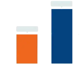
10.43 Billion
USD
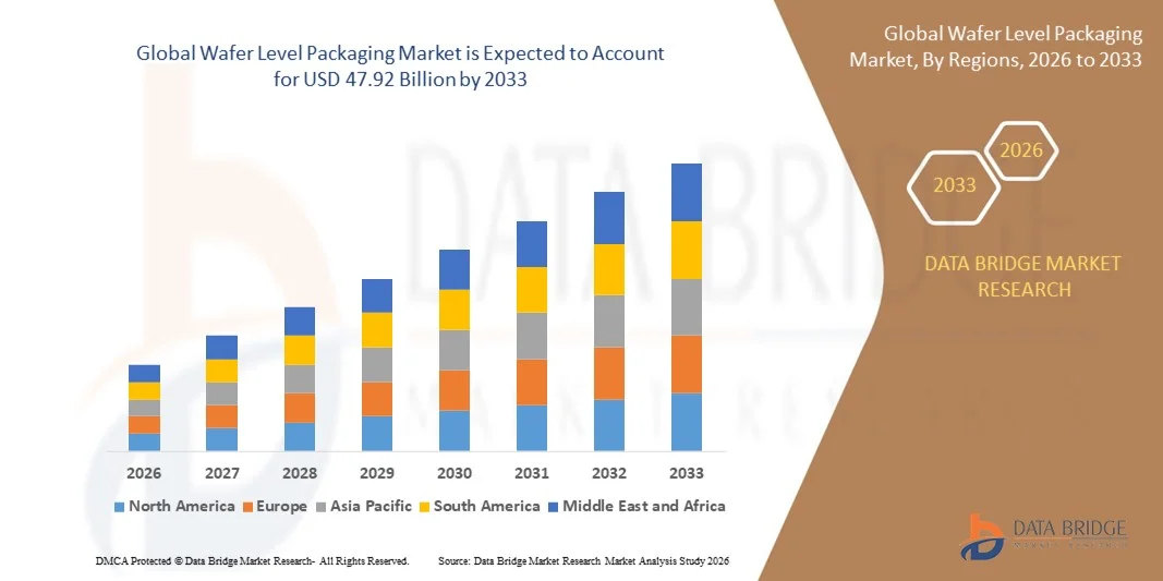
47.92 Billion
2025
2033
USD
10.43 Billion
USD
47.92 Billion
2025
2033
| 2026 - 2033 | |
| USD 10.43 Billion | |
| USD 47.92 Billion | |
| % | |
|
Wafer Level Packaging Market Size
- The global wafer level packaging market size was valued at USD 10.43 billion in 2025 and is expected to reach USD 47.92 billion by 2033, at a CAGR of 21.0% during the forecast period
- The market growth is largely fueled by the increasing demand for compact, high-performance, and energy-efficient semiconductor devices across consumer electronics, automotive, and industrial applications, encouraging manufacturers to adopt advanced wafer-level packaging methods to enhance functionality and reduce form factor
- Furthermore, rising production of smartphones, wearables, and IoT devices is accelerating the need for improved thermal performance, higher input/output density, and superior electrical characteristics, making wafer-level packaging an essential technology for next-generation electronic systems
Wafer Level Packaging Market Analysis
- Wafer level packaging, which enables the integration of multiple functions at the wafer stage, is becoming a critical technology for modern semiconductor manufacturing due to its ability to deliver higher miniaturization, improved reliability, and enhanced electrical performance for a wide range of end-use devices
- The escalating demand for wafer level packaging is primarily driven by rapid advancements in mobile communication, sensor technologies, and AI-enabled electronics, paired with the global shift toward smaller, faster, and more efficient semiconductor components needed across consumer, automotive, and industrial sectors
- Asia-Pacific dominated the wafer level packaging market with a share of 52.5% in 2025, due to the strong presence of semiconductor fabrication hubs, rising adoption of advanced packaging in consumer electronics, and expanding manufacturing ecosystems across major economies
- North America is expected to be the fastest growing region in the wafer level packaging market during the forecast period due to rising demand for high-performance semiconductors in consumer electronics, data centers, automotive electronics, and AI-driven devices
- Integrated passive device segment dominated the market with a market share in 2025, due to its growing adoption in smartphones, wearables, and RF applications requiring miniaturized, high-performance components. IPDs enable superior electrical performance, reduced parasitics, and enhanced signal integrity, making them essential in high-frequency communication devices. Their ability to consolidate multiple passive functions into a compact footprint drives strong adoption across consumer electronics and wireless modules. Manufacturers also prefer IPDs because they support high-volume production with excellent cost efficiency. Increasing integration of advanced communication standards such as 5G further boosts demand for IPD-based WLP solutions in compact electronic architectures
Report Scope and Wafer Level Packaging Market Segmentation
|
Attributes |
Wafer Level Packaging Key Market Insights |
|
Segments Covered |
|
|
Countries Covered |
North America
Europe
Asia-Pacific
Middle East and Africa
South America
|
|
Key Market Players |
|
|
Market Opportunities |
|
|
Value Added Data Infosets |
In addition to the insights on market scenarios such as market value, growth rate, segmentation, geographical coverage, and major players, the market reports curated by the Data Bridge Market Research also include import export analysis, production capacity overview, production consumption analysis, price trend analysis, climate change scenario, supply chain analysis, value chain analysis, raw material/consumables overview, vendor selection criteria, PESTLE Analysis, Porter Analysis, and regulatory framework. |
Wafer Level Packaging Market Trends
Rising Adoption of Advanced Fan-Out and 3D Wafer Level Packaging Technologies
- The wafer level packaging market is experiencing a strong shift toward advanced fan-out and 3D architectures as manufacturers prioritize higher performance and greater integration density for next-generation semiconductor devices. This trend is being shaped by the rising need for improved electrical performance, thinner form factors, and enhanced thermal efficiency across applications such as smartphones, high-performance computing, and automotive electronics
- For instance, Deca Technologies has expanded its fan-out packaging capabilities to support leading semiconductor manufacturers seeking higher throughput and improved design flexibility for complex chip architectures, demonstrating how industry players are accelerating innovation through scalable fan-out platforms
- Fan-out and 3D wafer level packaging enable shorter interconnects, higher I/O density, and improved system-in-package integration, making them essential for advanced processors, AI accelerators, and edge computing devices that require compact designs with strong power efficiency. This shift is further driven by increasing manufacturing optimization to enhance performance while controlling cost
- The demand for heterogeneous integration is supporting the adoption of these advanced WLP approaches as chipmakers integrate multiple functions such as memory, logic, and RF components within compact packages. This trend is also driven by the need to support the scaling limits of traditional 2D architectures
- Companies are focusing on expanding production capabilities and strengthening R&D for next-generation packaging technologies, which is accelerating the adoption of fan-out and 3D structures across various microelectronics applications. This focus is transforming expectations for performance and miniaturization in semiconductor packaging
- The rising emphasis on achieving higher system functionality in smaller footprints is pushing manufacturers toward advanced wafer level packaging, concluding the trend with strong momentum for continued adoption across consumer electronics, automotive, and high-performance computing markets
Wafer Level Packaging Market Dynamics
Driver
Growing Demand for Miniaturized and High-Performance Semiconductor Devices
- The increasing consumer and industrial demand for compact, power-efficient, and high-performance semiconductor devices is driving strong adoption of wafer level packaging solutions across multiple applications. As electronic devices become smaller and more advanced, WLP provides the density, speed, and reliability required for modern chip architectures
- For instance, Amkor Technology continues expanding its advanced wafer level packaging portfolio to meet the growing needs of smartphone manufacturers and computing device makers requiring thinner profiles and higher functional performance
- Miniaturization trends in consumer electronics such as wearables, IoT nodes, and smartphones are fueling demand for packaging solutions that can deliver high I/O density, enhanced signal integrity, and reduced latency. WLP enables these capabilities by minimizing interconnect length and optimizing the electrical path within the chip package
- Growing expectations for low-power consumption and enhanced device functionality are driving manufacturers to adopt wafer level packaging as a preferred integration solution across both consumer and industrial applications. This reinforces its critical role in next-generation semiconductor development
- The surge in demand for high-performance computing and compact electronics continues to position WLP as an essential technology, concluding this driver with its importance in enabling chip miniaturization and performance advancements
Restraint/Challenge
High Capital Investment and Complex Manufacturing Requirements
- The wafer level packaging market faces significant challenges due to the high capital investment required for advanced manufacturing infrastructure and the complexity of associated production processes. Establishing WLP fabrication lines demands costly equipment, precision tools, and specialized cleanroom environments, creating barriers for new entrants and smaller players
- For instance, companies investing in cutting-edge lithography, bonding, and metrology tools face substantial financial commitments, which can limit their ability to scale capacity rapidly. Advanced WLP processes such as fan-out, 3D stacking, and heterogeneous integration require intricate manufacturing expertise, precise alignment, and advanced material handling techniques, which increases operational complexity. These requirements make process optimization a major challenge for many semiconductor packaging facilities
- The need for ongoing investment in R&D, process automation, and quality assurance further elevates cost pressures, especially as packaging technologies evolve to support higher integration levels and finer feature sizes. This complexity slows adoption among cost-sensitive manufacturers
- As production technologies advance, maintaining yield stability and process uniformity becomes increasingly difficult due to multiple manufacturing steps and higher risks of defects, contributing to operational challenges. These issues affect scalability and cost efficiency
- The combination of high capital expenditure requirements and complex fabrication workflows presents a continuing challenge for wider adoption, concluding this section with the importance of addressing cost, capability, and manufacturing expertise constraints in WLP expansion
Wafer Level Packaging Market Scope
The market is segmented on the basis of integration, technology, application, and bumping technology.
- By Integration
On the basis of integration, the wafer level packaging market is segmented into Integrated Passive Device (IPD), Fan-In WLP, Fan-Out WLP, and Through-Silicon Via (TSV). The Integrated Passive Device segment dominated the market in 2025 due to its growing adoption in smartphones, wearables, and RF applications requiring miniaturized, high-performance components. IPDs enable superior electrical performance, reduced parasitics, and enhanced signal integrity, making them essential in high-frequency communication devices. Their ability to consolidate multiple passive functions into a compact footprint drives strong adoption across consumer electronics and wireless modules. Manufacturers also prefer IPDs because they support high-volume production with excellent cost efficiency. Increasing integration of advanced communication standards such as 5G further boosts demand for IPD-based WLP solutions in compact electronic architectures.
The Fan-Out WLP segment is expected to witness the fastest growth from 2026 to 2033, driven by its suitability for applications requiring high I/O density and improved thermal and electrical performance. Fan-Out WLP enables redistribution of connections, allowing more complex packaging while maintaining a thin profile, which makes it popular in next-generation mobile processors and power management ICs. The technology is increasingly adopted in advanced driver-assistance systems (ADAS), compact wearable electronics, and IoT modules that demand efficient heat dissipation and superior reliability. Its scalability for heterogeneous integration positions it strongly within evolving semiconductor designs. Continuous developments by major semiconductor companies to expand Fan-Out capacity further fuel its high growth trajectory during the forecast period.
- By Technology
On the basis of technology, the market is segmented into Flip Chip, Compliant WLP, Conventional Chip Scale Package, Wafer Level Chip Scale Package (WLCSP), Nano WLP, and 3D WLP. The WLCSP segment dominated the market in 2025 owing to its widespread adoption in mobile, consumer electronics, and automotive sensors requiring ultra-compact form factors. WLCSP delivers benefits such as low inductance, excellent thermal characteristics, high reliability, and true chip-size packaging, making it highly preferred for high-volume manufacturing. The technology supports efficient electrical characteristics critical for RF, power management, and MEMS devices. WLCSP also reduces processing steps and packaging cost, driving large-scale integration by leading semiconductor manufacturers. Its compatibility with advanced nodes ensures continued dominance in miniaturized electronics.
The 3D wafer level packaging segment is projected to register the fastest growth through 2033 due to the rising need for advanced stacking architectures that enhance performance and bandwidth. This technology supports vertical integration of dies, enabling shorter interconnects and higher processing speeds, which is crucial for HPC, AI accelerators, and next-generation memory devices. 3D WLP provides exceptional scalability for complex semiconductor designs requiring higher functionality within compact sizes. Growing adoption of 3D integration in data centers, high-performance consumer electronics, and automotive electronics accelerates its deployment. Continuous advancements in through-silicon via and hybrid bonding technologies strengthen the role of 3D WLP in the semiconductor packaging ecosystem.
- By Application
On the basis of application, the wafer level packaging market is segmented into Electronics, IT & Telecommunication, Industrial, Automotive, Aerospace & Defence, Healthcare, and Others. The Electronics segment dominated the market in 2025, driven by the massive consumption of smartphones, wearables, tablets, and AR/VR devices that require compact, high-performance semiconductor packages. Increasing adoption of miniaturized integrated circuits and sensors in consumer electronics further strengthens WLP demand. The segment benefits significantly from the need for low-power, thermally efficient, and cost-effective chips in portable electronics. WLP technologies enable enhanced functionality in limited board space, supporting manufacturers in delivering sleeker and high-performance devices. Continuous innovation in consumer gadgets globally ensures the electronics segment maintains its leadership position.
The automotive segment is anticipated to witness the fastest growth from 2026 to 2033 due to increasing electronic content in modern vehicles, including ADAS, infotainment systems, power electronics, and electric vehicle platforms. Automotive applications demand high-reliability, robust packaging solutions capable of withstanding extreme temperatures and vibration levels, making WLP an attractive choice. The shift toward vehicle electrification and autonomous mobility requires advanced semiconductor components that deliver superior efficiency and processing performance. WLP supports compact integration of sensors, microcontrollers, and power management ICs essential in next-generation automotive architectures. Growing investments by automotive OEMs and Tier-1 suppliers in advanced semiconductor technologies further accelerate the segment’s growth.
- By Bumping Technology
On the basis of bumping technology, the market is segmented into Copper Pillar, Solder Bumping, Gold Bumping, and Others. The Solder Bumping segment dominated the market in 2025 due to its maturity, cost-effectiveness, and widespread use across a variety of semiconductor devices. Solder bumps provide reliable electrical and mechanical connections for flip-chip and wafer-level packaging, making them ideal for high-volume manufacturing. The method supports strong thermal characteristics and compatibility with diverse applications, including mobile processors, memory, and RF components. Its long-established supply chain and manufacturing infrastructure further solidify its leading position. The technology remains a preferred choice for balancing performance, cost, and manufacturing efficiency in mainstream semiconductor production.
The Copper Pillar segment is projected to record the fastest growth during the forecast period due to its superior current-carrying capability, improved thermal performance, and fine-pitch scalability. Copper pillar bumping is increasingly deployed in high-density and high-performance devices such as advanced logic chips, AI processors, and high-bandwidth memory. The technology supports thinner interconnects and better electromigration resistance, making it suitable for modern compact semiconductor architectures. As advanced packaging methods such as 2.5D and 3D integration expand, copper pillar bumping becomes more critical. Rising adoption in automotive electronics, data centers, and premium consumer electronics accelerates its growth momentum through 2033.
Wafer Level Packaging Market Regional Analysis
- Asia-Pacific dominated the wafer level packaging market with the largest revenue share of 52.5% in 2025, driven by the strong presence of semiconductor fabrication hubs, rising adoption of advanced packaging in consumer electronics, and expanding manufacturing ecosystems across major economies
- The region’s cost-effective production capabilities, increasing investments in wafer-level technologies, and rapid growth in mobile device and IoT hardware manufacturing are accelerating overall market expansion
- The availability of skilled engineering talent, supportive government initiatives for semiconductor development, and large-scale electronics consumption across emerging economies are contributing to substantial adoption of wafer level packaging
China Wafer Level Packaging Market Insight
China held the largest share in the Asia-Pacific wafer level packaging market in 2025, owing to its dominant position in semiconductor assembly, testing, and consumer electronics production. The country's expanding foundry capabilities, strong government backing through semiconductor self-reliance programs, and growing focus on advanced packaging technologies are key growth drivers. Demand is further supported by large-scale production of smartphones, wearables, and high-performance processors for domestic and global markets.
India Wafer Level Packaging Market Insight
India is witnessing the fastest growth in the Asia-Pacific region, fueled by rising investments in semiconductor assembly and testing facilities, increasing demand for advanced packaging in smartphones and automotive electronics, and government-driven semiconductor manufacturing incentives. The “Make in India” initiative and growing interest from global chip manufacturers are strengthening adoption of wafer level packaging. Expansion of domestic electronics manufacturing and rapid growth in consumer device consumption are contributing to strong market momentum.
Europe Wafer Level Packaging Market Insight
The Europe wafer level packaging market is expanding steadily, supported by strong demand for advanced semiconductor solutions in automotive electronics, industrial automation, and high-reliability applications. The region emphasizes high-quality manufacturing, stringent regulatory standards, and technological advancement in high-performance microelectronics. Increasing adoption of miniaturized devices, ongoing R&D investments, and the rising need for efficient packaging for sensors and power electronics are further enhancing market growth.
Germany Wafer Level Packaging Market Insight
Germany’s wafer level packaging market is driven by its leadership in automotive electronics, advanced industrial machinery, and precision semiconductor manufacturing. The country’s strong R&D infrastructure, collaborations between academic research centers and semiconductor companies, and demand for high-reliability components in automotive and industrial applications are key contributors. Growing integration of sensors, power devices, and microcontrollers in next-generation vehicles supports the adoption of advanced packaging.
U.K. Wafer Level Packaging Market Insight
The U.K. market is supported by a mature electronics design ecosystem, ongoing efforts to strengthen semiconductor supply chain resilience, and rising investments in advanced research for microelectronics and nano-fabrication. Strong academic-industry collaboration, growth in medical electronics innovation, and focus on high-value semiconductor development continue to reinforce the U.K.’s role in specialized packaging technologies. Demand is particularly strong in life sciences instrumentation, communication devices, and industrial systems.
North America Wafer Level Packaging Market Insight
North America is projected to grow at the fastest CAGR from 2026 to 2033, driven by rising demand for high-performance semiconductors in consumer electronics, data centers, automotive electronics, and AI-driven devices. The region benefits from cutting-edge R&D capabilities, strong presence of leading fabless semiconductor companies, and rapid adoption of 3D and advanced wafer packaging technologies. Increasing reshoring of semiconductor manufacturing and major federal investments in chip fabrication are also accelerating market expansion.
U.S. Wafer Level Packaging Market Insight
The U.S. accounted for the largest share in the North America wafer level packaging market in 2025, supported by its strong semiconductor innovation ecosystem, advanced packaging R&D programs, and significant manufacturing capacity for high-performance computing, communication devices, and automotive electronics. The country’s emphasis on technological leadership, robust investment in chip design, and presence of major semiconductor manufacturers and foundries contribute to strong demand for wafer level packaging. The growing integration of AI, cloud computing, and EV electronics further strengthens the U.S. position in the regional market.
Wafer Level Packaging Market Share
The wafer level packaging industry is primarily led by well-established companies, including:
- JCET Group Co., Ltd. (China)
- NEMOTEK Technologie (Morocco)
- Chipbond Technology Corporation (Taiwan)
- Fujitsu (Japan)
- Powertech Technology Inc. (Taiwan)
- China Wafer Level CSP Co., Ltd. (China)
- Siliconware Precision Industries Co., Ltd. (Taiwan)
- Amkor Technology (U.S.)
- IQE PLC (U.K.)
- ChipMOS Technologies Inc. (Taiwan)
- Deca Technologies (U.S.)
- Qualcomm Technologies, Inc. (U.S.)
- Toshiba Corporation (Japan)
- Tokyo Electron Limited (Japan)
- Applied Materials, Inc. (U.S.)
- Lam Research Corporation (U.S.)
- ASML (Netherlands)
- Infineon Technologies AG (Germany)
- KLA Corporation (U.S.)
- Marvell (U.S.)
Latest Developments in Global Wafer Level Packaging Market
- In September 2024, Samsung Electronics announced a major expansion of its advanced packaging ecosystem by integrating enhanced wafer-level packaging and chiplet assembly capabilities into its South Korea manufacturing facilities. This initiative strengthens its position in heterogeneous integration, supports rising demand for high-density semiconductor packaging in AI and HPC applications, and accelerates the adoption of next-generation WLP technologies by improving production efficiency and reducing development cycles
- In August 2024, ASE Technology Holding revealed plans to upgrade its Taiwan manufacturing units with next-generation wafer-level testing platforms and advanced automation systems. This investment enhances production stability, supports higher volumes of compact and reliable WLP solutions, and strengthens the company’s capability to meet increasing demand from automotive electronics, IoT devices, and advanced consumer applications
- In March 2024, Arizona State University and Deca Technologies partnered to establish North America’s first dedicated research and development center for fan-out wafer-level packaging. This collaboration elevates U.S. technological leadership in advanced packaging, accelerates innovation in FOWLP architectures, and supports domestic semiconductor supply chain resilience by fostering industry-academic development of next-generation processes
- In March 2024, Taiwan Semiconductor Manufacturing Company Limited announced its plan to expand advanced chip packaging capacity in Japan as part of its broader global scaling strategy. This expansion improves regional manufacturing capability, strengthens supply chain diversification, and supports growing demand for wafer-level packaging technologies used in high-performance devices and advanced logic applications
- In June 2023, Onto Innovation launched its Applications Center of Excellence for panel-level packaging at its Wilmington, Massachusetts headquarters. This facility provides customers with direct access to equipment, software, and collaborative process environments that accelerate technology roadmaps, enhance PLP and WLP process optimization, and shorten time-to-yield for advanced semiconductor packaging solutions
SKU-
- Interactive Data Analysis Dashboard
- Company Analysis Dashboard for high growth potential opportunities
- Research Analyst Access for customization & queries
- Competitor Analysis with Interactive dashboard
- Latest News, Updates & Trend analysis
- Harness the Power of Benchmark Analysis for Comprehensive Competitor Tracking
Global Wafer Level Packaging Market, Supply Chain Analysis and Ecosystem Framework
To support market growth and help clients navigate the impact of geopolitical shifts, DBMR has integrated in-depth supply chain analysis into its Global Wafer Level Packaging Market research reports. This addition empowers clients to respond effectively to global changes affecting their industries. The supply chain analysis section includes detailed insights such as Global Wafer Level Packaging Market consumption and production by country, price trend analysis, the impact of tariffs and geopolitical developments, and import and export trends by country and HSN code. It also highlights major suppliers with data on production capacity and company profiles, as well as key importers and exporters. In addition to research, DBMR offers specialized supply chain consulting services backed by over a decade of experience, providing solutions like supplier discovery, supplier risk assessment, price trend analysis, impact evaluation of inflation and trade route changes, and comprehensive market trend analysis.
Data collection and base year analysis are done using data collection modules with large sample sizes. The stage includes obtaining market information or related data through various sources and strategies. It includes examining and planning all the data acquired from the past in advance. It likewise envelops the examination of information inconsistencies seen across different information sources. The market data is analysed and estimated using market statistical and coherent models. Also, market share analysis and key trend analysis are the major success factors in the market report. To know more, please request an analyst call or drop down your inquiry.
The key research methodology used by DBMR research team is data triangulation which involves data mining, analysis of the impact of data variables on the market and primary (industry expert) validation. Data models include Vendor Positioning Grid, Market Time Line Analysis, Market Overview and Guide, Company Positioning Grid, Patent Analysis, Pricing Analysis, Company Market Share Analysis, Standards of Measurement, Global versus Regional and Vendor Share Analysis. To know more about the research methodology, drop in an inquiry to speak to our industry experts.
Data Bridge Market Research is a leader in advanced formative research. We take pride in servicing our existing and new customers with data and analysis that match and suits their goal. The report can be customized to include price trend analysis of target brands understanding the market for additional countries (ask for the list of countries), clinical trial results data, literature review, refurbished market and product base analysis. Market analysis of target competitors can be analyzed from technology-based analysis to market portfolio strategies. We can add as many competitors that you require data about in the format and data style you are looking for. Our team of analysts can also provide you data in crude raw excel files pivot tables (Fact book) or can assist you in creating presentations from the data sets available in the report.


