
Middle East Africa Atomic Layer Deposition Market
Market Size in USD Million
CAGR :
% 
 USD
180.44 Million
USD
466.27 Million
2025
2033
USD
180.44 Million
USD
466.27 Million
2025
2033
| 2026 –2033 | |
| USD 180.44 Million | |
| USD 466.27 Million | |
| % | |
|
Atomic Layer Deposition Market Size
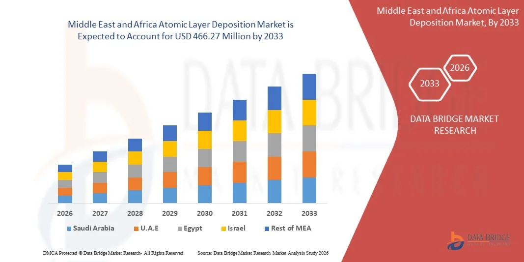
- The Middle East and Africa atomic layer deposition market size was valued at USD 180.44 million in 2025 and is expected to reach USD 466.27 million by 2033, at a CAGR of 12.6% during the forecast period
- The market growth is largely fueled by the rapid scaling of semiconductor manufacturing and the increasing demand for advanced nanoscale device fabrication, where atomic layer deposition enables ultra-precise thin-film control and uniform coating at atomic levels
- Furthermore, continuous technological advancements in deposition processes such as plasma-enhanced ALD and thermal ALD are improving film quality, process efficiency, and compatibility with complex 3D architectures, thereby accelerating adoption across next-generation electronics and high-performance computing applications
Atomic Layer Deposition Market Analysis
- Atomic layer deposition, enabling highly controlled, layer-by-layer material deposition, is becoming a critical enabling technology in semiconductor fabrication, solar devices, and advanced electronics due to its ability to deliver conformal coatings with exceptional thickness precision and material uniformity
- The rising demand for miniaturized electronic components, increasing adoption of advanced chip architectures such as FinFET and 3D NAND, and expanding applications in energy storage, optics, and medical devices are collectively driving strong market growth for atomic layer deposition technologies
- South Africa dominated the atomic layer deposition market in 2025, due to its relatively developed research ecosystem, growing electronics manufacturing activities, and increasing adoption of advanced material processing technologies across semiconductor, energy, and industrial applications
- Saudi Arabia is expected to be the fastest growing country in the atomic layer deposition market during the forecast period due to rapid industrial diversification under Vision 2030, strong investments in semiconductor-related technologies, and expanding focus on advanced manufacturing capabilities
- Aluminium Oxide ALD segment dominated the market with a market share of 39.1% in 2025, due to its extensive use as a high-quality dielectric and passivation layer in semiconductor and electronics manufacturing. Its superior conformality, excellent insulation properties, and strong chemical stability make it a preferred choice for thin-film coatings in advanced nodes and complex device architectures
Report Scope and Atomic Layer Deposition Market Segmentation
|
Attributes |
Atomic Layer Deposition Key Market Insights |
|
Segments Covered |
|
|
Countries Covered |
Middle East and Africa · Saudi Arabia · U.A.E. · South Africa · Egypt · Israel · Rest of Middle East and Africa |
|
Key Market Players |
|
|
Market Opportunities |
· Expansion in Next-Generation Memory Devices Such as 3D NAND and DRAM Manufacturing · Growing Application in Energy Storage Systems Including Lithium-Ion Batteries and Solid-State Batteries |
|
Value Added Data Infosets |
In addition to the insights on market scenarios such as market value, growth rate, segmentation, geographical coverage, and major players, the market reports curated by the Data Bridge Market Research also include import export analysis, production capacity overview, production consumption analysis, price trend analysis, climate change scenario, supply chain analysis, value chain analysis, raw material/consumables overview, vendor selection criteria, PESTLE Analysis, Porter Analysis, and regulatory framework. |
Atomic Layer Deposition Market Trends
“Integration of ALD in Advanced Semiconductor Nodes and 3D Architectures”
- A significant trend in the atomic layer deposition market is the increasing integration of ALD processes in advanced semiconductor nodes and complex 3D device architectures, driven by the need for ultra-thin, conformal, and defect-free film deposition at nanoscale dimensions. This integration is strengthening ALD’s role as a critical enabling technology for next-generation chip fabrication in logic and memory applications
- For instance, Intel and TSMC utilize ALD techniques in advanced process nodes for precise gate dielectric and spacer formation in FinFET and GAA transistor architectures. Such applications enhance device performance and support continued semiconductor scaling in high-performance computing and mobile electronics
- The adoption of ALD in 3D NAND and advanced memory structures is expanding as manufacturers require highly uniform layer deposition in vertically stacked cell designs. This is improving storage density and enabling continued innovation in high-capacity memory solutions
- The use of ALD in emerging applications such as compound semiconductors and photonic devices is increasing, supporting improved material quality and interface control. This is driving adoption in optoelectronics and high-frequency communication components
- Industries focusing on miniaturized electronics are increasingly relying on ALD to achieve atomic-level thickness control and improved reliability in thin-film coatings. This is strengthening its relevance in microelectronics manufacturing ecosystems
- The market is witnessing steady expansion of ALD equipment usage across semiconductor fabrication facilities as demand for advanced patterning and scaling solutions continues to rise. This ongoing shift is reinforcing ALD as a core deposition technology in modern electronics manufacturing
Atomic Layer Deposition Market Dynamics
Driver
“Rising Demand for Miniaturized High-Performance Electronics”
- The rising demand for miniaturized high-performance electronic devices is driving the adoption of atomic layer deposition due to its ability to deliver precise nanoscale coatings essential for advanced semiconductor performance. This demand is fueled by applications in smartphones, AI processors, and high-density computing systems requiring enhanced efficiency and power optimization
- For instance, Lam Research provides ALD equipment used in semiconductor fabrication for producing ultra-thin dielectric and conductive layers in advanced integrated circuits. These solutions support device scaling while maintaining electrical performance and reliability in complex chip designs
- The growing penetration of consumer electronics and wearable devices is increasing the need for compact components with high functional density and thermal stability. ALD processes enable material uniformity that supports these miniaturization requirements across semiconductor manufacturing
- The expansion of AI, 5G, and edge computing technologies is intensifying the requirement for faster and more efficient chips, further boosting ALD adoption in advanced fabrication nodes. These technologies rely on precise material engineering to enhance processing speed and energy efficiency
- The continuous evolution toward smaller, faster, and more energy-efficient electronic systems is reinforcing the need for ALD in next-generation device manufacturing. This sustained demand is strengthening its position as a key enabler of semiconductor innovation
Restraint/Challenge
“High Cost and Process Complexity”
- The atomic layer deposition market faces challenges due to the high cost of equipment and the complexity of maintaining precise process control at atomic scale, which requires advanced vacuum systems and specialized precursors. These factors increase capital investment requirements and limit adoption among cost-sensitive manufacturers
- For instance, Beneq develops ALD systems that require highly controlled reaction environments and specialized precursor delivery mechanisms to achieve uniform thin-film deposition. Such technical complexity increases system costs and requires skilled operation and maintenance expertise
- The need for extremely slow deposition cycles in ALD compared to other thin-film technologies results in lower throughput, which impacts production efficiency in high-volume manufacturing environments. This creates challenges in scaling ALD for mass production applications
- The requirement for high-purity chemicals and controlled processing conditions increases operational expenses and supply chain dependency on specialized materials. This adds further cost pressure on semiconductor manufacturers adopting ALD technologies
- The combination of high capital investment, operational complexity, and limited throughput continues to restrain widespread adoption of ALD technology. This reinforces cost optimization and process innovation as key priorities for market expansion
Atomic Layer Deposition Market Scope
The market is segmented on the basis of product type and application.
- By Product Type
On the basis of product type, the Atomic Layer Deposition market is segmented into Metal ALD, Aluminium Oxide ALD, Plasma Enhanced ALD, Catalytic ALD, and Others. The Aluminium Oxide ALD segment dominated the market with the largest market revenue share of 39.1% in 2025, driven by its extensive use as a high-quality dielectric and passivation layer in semiconductor and electronics manufacturing. Its superior conformality, excellent insulation properties, and strong chemical stability make it a preferred choice for thin-film coatings in advanced nodes and complex device architectures. The segment benefits from widespread adoption in memory devices, logic chips, and display technologies where precise thickness control is critical. Increasing demand for miniaturized and high-performance electronic components further strengthens its dominance. In addition, its cost-effectiveness and mature process integration capabilities support large-scale industrial deployment across multiple applications.
The Plasma Enhanced ALD segment is anticipated to witness the fastest growth rate from 2026 to 2033, fueled by its ability to enable low-temperature deposition and improved film quality compared to conventional thermal ALD processes. This technology is gaining traction in applications requiring enhanced film density, better step coverage, and faster deposition rates, particularly in next-generation semiconductor devices and flexible electronics. Its capability to deposit high-quality films on temperature-sensitive substrates makes it suitable for emerging applications such as OLED displays and advanced packaging. Growing demand for precision coatings in nanoscale devices and increasing investments in advanced manufacturing technologies accelerate its adoption. The continuous evolution of plasma-assisted techniques further enhances process efficiency and expands its application scope across industries.
- By Application
On the basis of application, the Atomic Layer Deposition market is segmented into Semiconductors, Solar Devices, Electronics, Medical Equipment, Research & Development Facilities, Fuel Cells, Optical Devices, Thermoelectric Materials, Magnetic Heads, Sensors, Barrier Layers, Primer Layers, Non—IC Application, and Others. The Semiconductors segment dominated the market with the largest market revenue share in 2025, driven by the critical role of ALD in fabricating ultra-thin, uniform films required for advanced integrated circuits. The increasing complexity of chip architectures, including 3D NAND, FinFET, and gate-all-around structures, relies heavily on ALD for precise material deposition at the atomic scale. Rising global demand for high-performance computing, AI chips, and memory devices continues to boost the adoption of ALD in semiconductor fabrication. The segment also benefits from continuous investments in foundries and the transition toward smaller process nodes. In addition, the need for defect-free and highly reliable components reinforces the importance of ALD technologies in semiconductor manufacturing.
The Solar Devices segment is expected to witness the fastest CAGR from 2026 to 2033, driven by the growing emphasis on renewable energy and the need to improve solar cell efficiency and durability. ALD is increasingly used for surface passivation and protective coatings in photovoltaic cells, enhancing energy conversion efficiency and extending operational lifespan. The rising adoption of advanced solar technologies such as thin-film and perovskite solar cells further accelerates demand for ALD processes. Increasing government initiatives supporting clean energy deployment and sustainability goals contribute to segment growth. Moreover, the ability of ALD to provide uniform coatings on complex structures makes it highly suitable for next-generation solar device manufacturing.
Atomic Layer Deposition Market Regional Analysis
- South Africa dominated the atomic layer deposition market with the largest revenue share in 2025, driven by its relatively developed research ecosystem, growing electronics manufacturing activities, and increasing adoption of advanced material processing technologies across semiconductor, energy, and industrial applications
- The presence of established academic and industrial research institutions such as the Council for Scientific and Industrial Research (CSIR) and collaborations with global semiconductor equipment suppliers supports early-stage adoption of ALD technologies in thin-film coatings, nanomaterials, and advanced surface engineering applications
- Rising investments in scientific research infrastructure, increasing focus on advanced materials development, and growing adoption of high-precision deposition techniques in electronics and energy sectors are accelerating ALD adoption
Saudi Arabia Atomic Layer Deposition Market Insight
Saudi Arabia is projected to register the fastest CAGR in the Middle East & Africa atomic layer deposition market from 2026 to 2033, supported by rapid industrial diversification under Vision 2030, strong investments in semiconductor-related technologies, and expanding focus on advanced manufacturing capabilities. Growing initiatives in electronics, energy storage, and renewable energy projects are driving demand for high-precision thin-film deposition solutions. Expanding collaboration with global technology providers and increasing establishment of research centers focused on nanotechnology and materials science are accelerating ALD adoption. Strong government support for localization of advanced manufacturing and technology transfer is further strengthening market development. Rising demand for high-performance electronic components in defense, telecom, and smart infrastructure is contributing to sustained market growth. Saudi Arabia’s strategic push toward technology-driven industrial transformation positions it as the fastest-growing market in the region.
U.A.E. Atomic Layer Deposition Market Insight
The U.A.E. is witnessing steady growth in the Middle East & Africa atomic layer deposition market, driven by its strong focus on advanced technology adoption, semiconductor research initiatives, and expansion of high-tech industrial ecosystems. Increasing investments in nanotechnology, electronics innovation, and renewable energy applications are supporting ALD usage in coatings, sensors, and advanced material development. The presence of world-class research institutions and innovation hubs such as Khalifa University and Technology Innovation Institute is strengthening capabilities in advanced materials science. Growing partnerships with global semiconductor and equipment manufacturers are further enhancing technology transfer and adoption. Expansion of aerospace, defense, and smart infrastructure projects is increasing demand for precision-engineered components. Continuous focus on diversification into knowledge-based industries reinforces the U.A.E.’s strong position in the regional market.
Atomic Layer Deposition Market Share
The atomic layer deposition industry is primarily led by well-established companies, including:
- ADEKA CORPORATION (Japan)
- AIXTRON SE (Germany)
- Applied Materials Inc. (U.S.)
- ASM International N.V. (Netherlands)
- LAM RESEARCH CORPORATION (U.S.)
- Tokyo Electron Limited (Japan)
- Kurt J. Lesker Company (U.S.)
- Beneq Oy (Finland)
- Veeco Instruments Inc. (U.S.)
- Encapsulix (France)
- SENTECH Instruments GmbH (Germany)
- Oxford Instruments plc (U.K.)
- Forge Nano Inc. (U.S.)
- Merck KGaA (Germany)
- HZO, Inc. (U.S.)
- Picosun Oy (Finland)
Latest Developments in Middle East and Africa Atomic Layer Deposition Market
- In January 2026, Applied Materials, Inc. introduced an advanced atomic layer deposition system designed for high-aspect-ratio structures in next-generation logic and memory chips, integrating selective ALD capabilities to enhance pattern precision and material efficiency. The system focuses on enabling defect-free deposition in increasingly complex chip architectures required for AI and high-performance computing applications. In conclusion, this development accelerates innovation in semiconductor scaling and strengthens Applied Materials’ competitive position in advanced deposition solutions while driving overall market growth
- In December 2025, ASM International N.V. launched an upgraded plasma-enhanced ALD platform optimized for low-temperature processing of advanced nodes and heterogeneous integration. The solution improves film uniformity and throughput while supporting deposition on temperature-sensitive materials used in advanced packaging and flexible electronics. In conclusion, this launch enhances manufacturing efficiency and broadens the adoption of ALD technologies across emerging electronics applications, reinforcing ASM International’s presence in the evolving deposition market
- In November 2025, Beneq Oy launched the Transmute ALD platform, an advanced next-generation deposition system developed for high-volume manufacturing of wide-bandgap power electronics, RF components, and micro-LED applications. The platform integrates plasma pretreatment, PEALD, and thermal ALD capabilities to ensure high-throughput production with precise atomic-level interface control. In conclusion, this launch strengthens Beneq’s position in advanced semiconductor deposition technologies and supports next-generation electronics manufacturing
- In September 2025, Forge Nano Inc. introduced its TEPHRA One 200 mm single-wafer ALD tool at SEMICON Taiwan, designed to support automated deposition of oxides, nitrides, and nanolaminate coatings for compound semiconductor fabrication. The system enables faster coating speeds and scalable wafer-level production for advanced electronics applications. In conclusion, this innovation enhances production efficiency and expands Forge Nano’s capabilities in semiconductor ALD solutions
- In February 2025, Lam Research Corporation unveiled the ALTUS Halo atomic layer deposition system, recognized as the industry’s first molybdenum ALD solution for high-volume semiconductor manufacturing. The platform delivers low-resistivity and void-free metallization essential for advanced memory and logic chips, supporting continued scaling for AI and next-generation devices. In conclusion, this development reinforces Lam Research’s leadership in precision semiconductor deposition technologies
SKU-
Get online access to the report on the World's First Market Intelligence Cloud
- Interactive Data Analysis Dashboard
- Company Analysis Dashboard for high growth potential opportunities
- Research Analyst Access for customization & queries
- Competitor Analysis with Interactive dashboard
- Latest News, Updates & Trend analysis
- Harness the Power of Benchmark Analysis for Comprehensive Competitor Tracking
Middle East Africa Atomic Layer Deposition Market, Supply Chain Analysis and Ecosystem Framework
To support market growth and help clients navigate the impact of geopolitical shifts, DBMR has integrated in-depth supply chain analysis into its Middle East Africa Atomic Layer Deposition Market research reports. This addition empowers clients to respond effectively to global changes affecting their industries. The supply chain analysis section includes detailed insights such as Middle East Africa Atomic Layer Deposition Market consumption and production by country, price trend analysis, the impact of tariffs and geopolitical developments, and import and export trends by country and HSN code. It also highlights major suppliers with data on production capacity and company profiles, as well as key importers and exporters. In addition to research, DBMR offers specialized supply chain consulting services backed by over a decade of experience, providing solutions like supplier discovery, supplier risk assessment, price trend analysis, impact evaluation of inflation and trade route changes, and comprehensive market trend analysis.
Research Methodology
Data collection and base year analysis are done using data collection modules with large sample sizes. The stage includes obtaining market information or related data through various sources and strategies. It includes examining and planning all the data acquired from the past in advance. It likewise envelops the examination of information inconsistencies seen across different information sources. The market data is analysed and estimated using market statistical and coherent models. Also, market share analysis and key trend analysis are the major success factors in the market report. To know more, please request an analyst call or drop down your inquiry.
The key research methodology used by DBMR research team is data triangulation which involves data mining, analysis of the impact of data variables on the market and primary (industry expert) validation. Data models include Vendor Positioning Grid, Market Time Line Analysis, Market Overview and Guide, Company Positioning Grid, Patent Analysis, Pricing Analysis, Company Market Share Analysis, Standards of Measurement, Global versus Regional and Vendor Share Analysis. To know more about the research methodology, drop in an inquiry to speak to our industry experts.
Customization Available
Data Bridge Market Research is a leader in advanced formative research. We take pride in servicing our existing and new customers with data and analysis that match and suits their goal. The report can be customized to include price trend analysis of target brands understanding the market for additional countries (ask for the list of countries), clinical trial results data, literature review, refurbished market and product base analysis. Market analysis of target competitors can be analyzed from technology-based analysis to market portfolio strategies. We can add as many competitors that you require data about in the format and data style you are looking for. Our team of analysts can also provide you data in crude raw excel files pivot tables (Fact book) or can assist you in creating presentations from the data sets available in the report.


