

What is the Advanced Packaging Inspection Systems Market Size and Growth Rate?
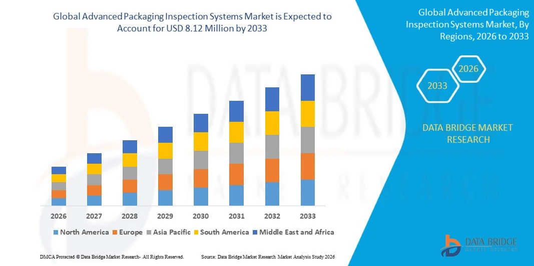
- As per Data Bridge Market Research analysis, the advanced packaging inspection systems market was valued at USD 3.5 Million in 2025 and is projected to reach USD 8.12 Million by 2033, growing at a CAGR of 11.10% from 2026 to 2033.
- The market is gaining momentum as semiconductor manufacturers scale advanced packaging architectures such as fan-out wafer-level packaging, 2.5D interposers, and 3D stacked dies, all of which require finer defect-detection tolerances than conventional back-end inspection can deliver.
- Rising demand for AI accelerators, high-bandwidth memory, and chiplet-based system architectures is compelling OSATs and foundries to adopt multi-mode optical, X-ray, and acoustic inspection platforms capable of resolving sub-micron interconnect defects across increasingly dense package structures.
Market Size & Forecast
- Global Market Value (2025): USD 3.5 Million
- Expected Market Value (2033): USD 8.12 Million
- Forecast CAGR (2026–2033): 11.10%
- Leading Region in 2025: Asia-Pacific
- Fastest Growing Region: North America
What are the Major Takeaways of the Advanced Packaging Inspection Systems Market?
- Asia-Pacific dominated the global advanced packaging inspection systems market with the largest revenue share of 38.60% in 2025, supported by the concentration of leading-edge packaging capacity across Taiwan, South Korea, and China and continued capital investment by foundries and OSATs.
- North America is expected to be the fastest-growing region at a CAGR of 12.90% from 2026 to 2033, fueled by incentive-driven expansion of domestic advanced packaging capacity and rising installation of inline inspection tools at new U.S. facilities.
- The automated optical inspection segment led the market with a 34.20% share in 2025, driven by its high throughput, non-contact operation, and established role in bump and redistribution-layer inspection across fan-out and flip chip lines.
- X-ray inspection is the fastest-growing inspection technique, projected to register a CAGR of 13.40%, reflecting rising adoption for hidden-defect detection in stacked die and through-silicon via structures that optical systems cannot resolve.
- The fan-out wafer-level packaging segment dominated the packaging type category with a 29.80% revenue share in 2025, led by its widespread use in mobile application processors, RF modules, and compact consumer devices.
- The 2.5D/3D IC packaging segment is expected to be the fastest-growing packaging type, projected to grow at a CAGR of 12.60%, driven by surging demand for AI accelerator and high-bandwidth memory packages.
- Inline deployment accounted for 61.40% of the market share in 2025, preferred by foundries and OSATs that require real-time process control to reduce yield loss on high-volume advanced packaging lines.
- The OSAT providers segment accounted for the largest share of 42.30% in 2025, reflecting their central role in providing outsourced advanced packaging and test services to fabless semiconductor companies globally, and their need to maintain high first-pass yield across diverse customer packaging designs.
Report Scope and Advanced Packaging Inspection Systems Market Segmentation
|
Attributes |
Advanced Packaging Inspection Systems Market Insights |
|
Segments Covered |
|
|
Countries Covered |
North America
Europe
Asia-Pacific
Middle East and Africa
South America
|
|
Key Market Players |
|
|
Market Opportunities |
|
|
Value Added Data Infosets |
In addition to the insights on market scenarios such as market value, growth rate, segmentation, geographical coverage, and major players, the market reports curated by the Data Bridge Market Research also include in-depth expert analysis, geographically represented company-wise production and capacity, network layouts of distributors and partners, detailed and updated price trend analysis and deficit analysis of supply chain and demand. |
What is the Key Trend in the Advanced Packaging Inspection Systems Market?
- Semiconductor manufacturers are increasingly deploying AI- and machine-learning-based defect classification within inspection workflows to improve first-pass detection accuracy while reducing manual review time on advanced packaging lines.
- For instance, in March 2025, Onto Innovation expanded its Dragonfly platform portfolio with enhanced hybrid optical metrology capabilities aimed at supporting high-volume manufacturing of 2.5D and 3D packaged devices for AI and high-performance computing applications.
- Inspection equipment suppliers are collaborating more closely with OSATs and foundries to co-develop recipe libraries for emerging bump and interconnect geometries, shortening qualification cycles for new packaging nodes.
- For instance, in June 2025, Camtek Ltd. introduced additional configurations of its Falcon inspection and metrology platform targeted at high-density fan-out and panel-level packaging processes, aimed at improving throughput for advanced packaging customers in Asia-Pacific.
- Equipment vendors are increasingly offering hybrid platforms that combine optical, X-ray, and acoustic modalities within a single inspection cell, allowing manufacturers to consolidate multiple defect-detection steps and reduce fab floor space requirements.
- For instance, in July 2025, Bruker Corporation expanded its X-ray metrology product line with additional throughput enhancements aimed at high-volume advanced packaging fabs transitioning to 3D stacked die architectures.
- Cloud-connected inspection platforms that centralize defect data across multiple fab sites are gaining traction, enabling OSATs with distributed manufacturing footprints to standardize quality control and accelerate root-cause analysis.
- For instance, in October 2025, CyberOptics Corporation released an updated version of its SQ3000 multi-reflection suppression sensor platform, aimed at improving 3D inspection accuracy for fine-pitch bump structures used in advanced packaging.
- Overall, the advanced packaging inspection systems market is moving toward intelligent, automated, and integrated inspection solutions that combine AI-driven defect classification, multi-modal metrology, high-throughput inspection, and centralized data analytics.
What are the Key Drivers of the Advanced Packaging Inspection Systems Market?
- The rapid transition toward chiplet-based system architectures and heterogeneous integration is significantly increasing the number of interconnects per package, raising the criticality of defect-free bump, redistribution-layer, and through-silicon via structures.
- For instance, in January 2025, KLA Corporation broadened its portfolio for advanced packaging process control, adding new e-beam and optical inspection capabilities positioned to support high-volume production of AI accelerator packages with sub-micron interconnect pitches.
- Growing capital expenditure by foundries and OSATs on advanced packaging capacity, supported by government semiconductor incentive programs in the U.S., the EU, and Asia-Pacific, is expanding the installed base of inspection systems.
- For instance, in September 2025, Amkor Technology announced continued expansion of its advanced packaging facility in Arizona, incorporating expanded automated inspection and metrology capacity to support 2.5D and fan-out packaging for U.S.-based customers.
- Rising demand for high-bandwidth memory and AI accelerator packages is pushing manufacturers toward tighter interconnect pitches, which in turn requires inspection systems with finer resolution and higher measurement repeatability.
- For instance, in April 2025, Onto Innovation announced an expanded collaboration with a leading memory manufacturer to deploy hybrid metrology tools across multiple high-bandwidth memory packaging lines, supporting yield ramp for next-generation AI memory products.
- Stricter quality and reliability requirements from automotive and data-center customers are compelling OSATs to adopt inline inspection earlier in the packaging process flow rather than relying solely on final electrical test.
What Factors Are Challenging the Growth of the Advanced Packaging Inspection Systems Market?
- Advanced packaging inspection systems require substantial upfront capital investment due to the precision optics, X-ray sources, and computing infrastructure needed to resolve sub-micron defects, limiting adoption among smaller OSATs and research fabs.
- For instance, in 2025, several mid-tier OSATs in Southeast Asia cited the high cost of qualifying new inline X-ray and acoustic inspection tools as a constraint on the pace at which they could scale advanced packaging capacity, illustrating the financial barrier smaller providers face relative to leading-edge foundries.
- The increasing complexity and diversity of packaging architectures also requires frequent recipe development and system recalibration, adding to the operating cost and slowing time-to-qualification for new inspection platforms.
- A shortage of process engineers trained in advanced packaging metrology and defect analysis is constraining the pace at which fabs can bring new inspection capacity online.
- For instance, in 2025, industry surveys of OSAT hiring trends noted persistent difficulty filling advanced packaging metrology engineer roles across Taiwan and Southeast Asia, underscoring the talent constraint facing equipment operators as inspection technology grows more complex.
- High capital investment and recurring calibration costs associated with advanced inspection systems continue to restrict adoption among smaller and mid-sized organizations, limiting the pace of technology diffusion in price-sensitive and emerging semiconductor packaging hubs.
How is the Advanced Packaging Inspection Systems Market Segmented?
The advanced packaging inspection systems market is segmented on the basis of inspection technique, packaging type, application, end user, and deployment.
- By Inspection Technique
On the basis of inspection technique, the global advanced packaging inspection systems market is segmented into automated optical inspection, X-ray inspection, scanning acoustic microscopy, electrical test inspection, and hybrid inspection systems. The automated optical inspection segment dominated the market with a 34.20% share in 2025, owing to its high throughput, non-destructive nature, and established use across bump, redistribution-layer, and surface-defect inspection in high-volume packaging lines. These systems deliver rapid, repeatable measurement without physically contacting the die, making them the preferred first line of defect detection for OSATs and foundries scaling fan-out and flip chip production.
The X-ray inspection segment is projected to register the fastest growth at a CAGR of 13.40% from 2026 to 2033, driven by rising demand for non-destructive detection of hidden defects such as voids, delamination, and incomplete solder joints in stacked die and through-silicon via structures that cannot be identified through surface-level optical methods. Advances in micro-focus and 3D computed tomography X-ray systems, combined with declining per-unit inspection costs, are accelerating segment expansion across advanced packaging fabs.
- By Packaging Type
On the basis of packaging type, the global advanced packaging inspection systems market is segmented into fan-out wafer-level packaging, 2.5D/3D IC packaging, flip chip packaging, system-in-package, and wafer-level chip-scale packaging. The fan-out wafer-level packaging segment held the leading share of 29.80% in 2025, supported by its extensive use in mobile application processors, RF modules, and compact consumer electronics, where its ability to deliver high input/output density without a silicon interposer keeps unit costs low for high-volume production.
The 2.5D/3D IC packaging segment is expected to grow at the fastest pace, registering a CAGR of 12.60% from 2026 to 2033, driven by increasing adoption in AI accelerators, high-bandwidth memory, and high-performance computing applications that require dense vertical and lateral interconnects. Rising capital investment by leading foundries in interposer-based packaging capacity is directly translating into higher demand for inspection tools capable of resolving micro-bump and through-silicon via defects.
- By Application
On the basis of application, the global advanced packaging inspection systems market is segmented into bump inspection, through-silicon via inspection, redistribution layer inspection, wire-bond inspection, and die-attach inspection. The bump inspection segment held the leading share of 31.50% in 2025, as bump-level defects such as voids, bridging, and height variation are among the most common yield-limiting issues across fan-out, flip chip, and wafer-level chip-scale packaging, making bump inspection a mandatory step in nearly every advanced packaging process flow.
The through-silicon via inspection segment is projected to register the fastest growth, at a CAGR of 13.10% from 2026 to 2033, as rising adoption of 2.5D and 3D IC packaging for AI accelerators and high-bandwidth memory increases the density and criticality of through-silicon via structures, which require specialized X-ray and acoustic inspection techniques to detect voids and incomplete fill that are invisible to surface-level methods.
- By End User
On the basis of end user, the global advanced packaging inspection systems market is segmented into integrated device manufacturers, outsourced semiconductor assembly and test providers, foundries, and research institutions. OSAT providers accounted for the largest share of 42.30% in 2025, reflecting their central role in providing outsourced advanced packaging and test services to fabless semiconductor companies globally, and their need to maintain high first-pass yield across diverse customer packaging designs.
Foundries are expected to be the fastest-growing end-user segment, registering a CAGR of 12.10%, as leading-edge foundries increasingly integrate advanced packaging and inspection directly into their front-end-adjacent process flows to support chiplet and heterogeneous integration offerings, reducing their dependence on external OSAT packaging partners for the most performance-critical products.
- By Deployment
On the basis of deployment, the global advanced packaging inspection systems market is segmented into inline inspection and offline/lab-based inspection. Inline inspection accounted for the larger share of 61.40% in 2025, as foundries and OSATs increasingly prioritize real-time process control positioned directly within the production line to catch defects early and reduce yield loss before packages advance to subsequent process steps.
Offline/lab-based inspection is expected to grow at a comparatively faster pace, registering a CAGR of 9.80% from 2026 to 2033, supported by rising demand for detailed failure analysis and process characterization at research institutions and foundry development labs as packaging architectures grow more complex and require deeper root-cause investigation than inline tools alone can provide.
Which Region Holds the Largest Share of the Advanced Packaging Inspection Systems Market?
- Asia-Pacific dominated the global advanced packaging inspection systems market and accounted for the largest revenue share of 38.60% in 2025, supported by the concentration of advanced packaging capacity in Taiwan, South Korea, China, and Singapore and sustained capital investment by leading foundries and OSATs.
- The region also benefits from proximity to major semiconductor fabrication clusters, established supply chains for inspection consumables and services, and continued government support for domestic semiconductor manufacturing capacity. Growing investment in AI accelerator and high-bandwidth memory packaging across Taiwan and South Korea continues to strengthen Asia-Pacific's leadership position in the global market.
U.K. Advanced Packaging Inspection Systems Market Insight
The U.K. advanced packaging inspection systems market is supported by the country’s growing semiconductor research and development activities, increasing focus on heterogeneous integration, and investments in advanced packaging technologies. Demand for high-precision inspection and metrology solutions is increasing as semiconductor research organizations, chip designers, and packaging facilities adopt more complex interconnect and miniaturized packaging structures. Furthermore, advancements in AI-enabled inspection, optical metrology, and automated defect detection are supporting the adoption of advanced inspection systems across semiconductor development and manufacturing applications.
Germany Advanced Packaging Inspection Systems Market Insight
The Germany advanced packaging inspection systems market is expanding due to the country’s strong semiconductor manufacturing ecosystem, established automotive electronics industry, and increasing investment in advanced semiconductor technologies. The growing adoption of chiplet-based architectures, heterogeneous integration, and high-density interconnects is increasing demand for precise inspection and metrology solutions. In addition, Germany’s strong industrial automation capabilities and focus on semiconductor research are supporting the integration of automated optical inspection, X-ray inspection, and AI-based defect detection technologies across advanced packaging processes.
Asia-Pacific Advanced Packaging Inspection Systems Market Insight
The Asia-Pacific advanced packaging inspection systems market is witnessing strong growth, driven by the region’s concentration of semiconductor foundries, OSATs, memory manufacturers, and advanced packaging facilities across Taiwan, South Korea, China, and Japan. Increasing investments in 2.5D and 3D packaging, chiplets, high-bandwidth memory, fan-out packaging, and high-density interconnect technologies are creating demand for high-throughput and high-precision inspection systems. Furthermore, the expansion of AI and high-performance computing semiconductor production is accelerating investments in automated optical, X-ray, metrology, and AI-enabled inspection technologies across the region.
Japan Advanced Packaging Inspection Systems Market Insight
The Japan advanced packaging inspection systems market is experiencing steady growth, supported by the country’s established semiconductor materials and equipment ecosystem, increasing investment in advanced packaging research, and growing demand for high-performance semiconductor components. Semiconductor manufacturers and research organizations are increasingly focusing on chiplet integration, 3D packaging, and high-density interconnect technologies, creating demand for sophisticated inspection and metrology solutions. Moreover, Japan’s strong capabilities in precision manufacturing, semiconductor equipment, and materials are supporting the development and adoption of advanced inspection technologies for next-generation packaging applications.
China Advanced Packaging Inspection Systems Market Insight
The China advanced packaging inspection systems market is expanding rapidly, supported by continued investment in domestic semiconductor manufacturing and packaging capabilities and increasing efforts to strengthen the local semiconductor supply chain. Growing adoption of advanced packaging technologies, including 2.5D, 3D, fan-out, and high-density interconnect structures, is increasing demand for automated inspection and metrology systems. In addition, rising investments in domestic semiconductor equipment and increasing adoption of AI-enabled defect detection are supporting the development of localized inspection capabilities across Chinese semiconductor manufacturing and packaging facilities.
Which are the Top Companies in Advanced Packaging Inspection Systems Market?
The advanced packaging inspection systems industry is primarily led by well-established companies, including:
- KLA Corporation (U.S.)
- Onto Innovation Inc. (U.S.)
- Camtek Ltd. (Israel)
- Semiconductor Technologies & Instruments Pte Ltd. (Singapore)
- Cohu, Inc. (U.S.)
- Nordson Corporation (U.S.)
- Bruker Corporation (U.S.)
- Test Research, Inc. (Taiwan)
- Viscom AG (Germany)
- CyberOptics Corporation (U.S.)
- SAKI Corporation (Japan)
- ASM International N.V. (Netherlands)
- Nearfield Instruments B.V. (Netherlands)
- TASMIT, Inc. (Japan)
- Shenzhen Skyverse Technology Co., Ltd. (China)
- Cheng Mei Instrument Technology Co., Ltd. (Taiwan)
- Koh Young Technology Inc. (South Korea)
What are Latest Developments in Advanced Packaging Inspection Systems Market?
- In March 2025, Onto Innovation expanded its Dragonfly hybrid metrology platform with additional capabilities for 2.5D and 3D advanced packaging process control, aimed at supporting high-volume manufacturing for AI and high-performance computing applications.
- In June 2025, Camtek Ltd. introduced new configurations of its Falcon inspection and metrology system targeted at high-density fan-out and panel-level packaging, aimed at improving throughput for advanced packaging customers in Asia-Pacific.
- In January 2025, KLA Corporation broadened its advanced packaging process control portfolio with new optical and e-beam inspection capabilities positioned for high-volume production of AI accelerator packages.
- In September 2025, Amkor Technology announced continued expansion of its advanced packaging facility in Arizona, incorporating additional automated inspection and metrology capacity to support 2.5D and fan-out packaging for U.S. customers.
- In February 2025, Camtek Ltd. launched its Hawk inspection and metrology platform for advanced packaging applications, including chiplets, high-bandwidth memory (HBM), and hybrid bonding. The system was designed to support detection of defects as small as 150 nanometers and measurement of up to 500 million microbumps at pitches below 12 microns.
- In April 2025, Camtek Ltd. received Intel’s 2025 EPIC Supplier Award, recognizing the company’s contribution to Intel’s manufacturing ecosystem and reflecting its growing role in advanced semiconductor inspection and metrology applications.
- In June 2025, Bruker Corporation announced the shipment and installation of its 15th InSight WLI 3D optical metrology system to a leading semiconductor manufacturer as part of a larger order for 27 systems during 2025. The systems support advanced packaging process steps for AI and high-performance computing chips.
- Interactive Data Analysis Dashboard
- Company Analysis Dashboard for high growth potential opportunities
- Research Analyst Access for customization & queries
- Competitor Analysis with Interactive dashboard
- Latest News, Updates & Trend analysis
- Harness the Power of Benchmark Analysis for Comprehensive Competitor Tracking
Global Advanced Packaging Inspection Systems Market, Supply Chain Analysis and Ecosystem Framework
To support market growth and help clients navigate the impact of geopolitical shifts, DBMR has integrated in-depth supply chain analysis into its Global Advanced Packaging Inspection Systems Market research reports. This addition empowers clients to respond effectively to global changes affecting their industries. The supply chain analysis section includes detailed insights such as Global Advanced Packaging Inspection Systems Market consumption and production by country, price trend analysis, the impact of tariffs and geopolitical developments, and import and export trends by country and HSN code. It also highlights major suppliers with data on production capacity and company profiles, as well as key importers and exporters. In addition to research, DBMR offers specialized supply chain consulting services backed by over a decade of experience, providing solutions like supplier discovery, supplier risk assessment, price trend analysis, impact evaluation of inflation and trade route changes, and comprehensive market trend analysis.
Data collection and base year analysis are done using data collection modules with large sample sizes. The stage includes obtaining market information or related data through various sources and strategies. It includes examining and planning all the data acquired from the past in advance. It likewise envelops the examination of information inconsistencies seen across different information sources. The market data is analysed and estimated using market statistical and coherent models. Also, market share analysis and key trend analysis are the major success factors in the market report. To know more, please request an analyst call or drop down your inquiry.
The key research methodology used by DBMR research team is data triangulation which involves data mining, analysis of the impact of data variables on the market and primary (industry expert) validation. Data models include Vendor Positioning Grid, Market Time Line Analysis, Market Overview and Guide, Company Positioning Grid, Patent Analysis, Pricing Analysis, Company Market Share Analysis, Standards of Measurement, Global versus Regional and Vendor Share Analysis. To know more about the research methodology, drop in an inquiry to speak to our industry experts.
Data Bridge Market Research is a leader in advanced formative research. We take pride in servicing our existing and new customers with data and analysis that match and suits their goal. The report can be customized to include price trend analysis of target brands understanding the market for additional countries (ask for the list of countries), clinical trial results data, literature review, refurbished market and product base analysis. Market analysis of target competitors can be analyzed from technology-based analysis to market portfolio strategies. We can add as many competitors that you require data about in the format and data style you are looking for. Our team of analysts can also provide you data in crude raw excel files pivot tables (Fact book) or can assist you in creating presentations from the data sets available in the report.