

Electronic Design Automation (EDA) Tools in Integrated Circuits (IC) Industry Market Size
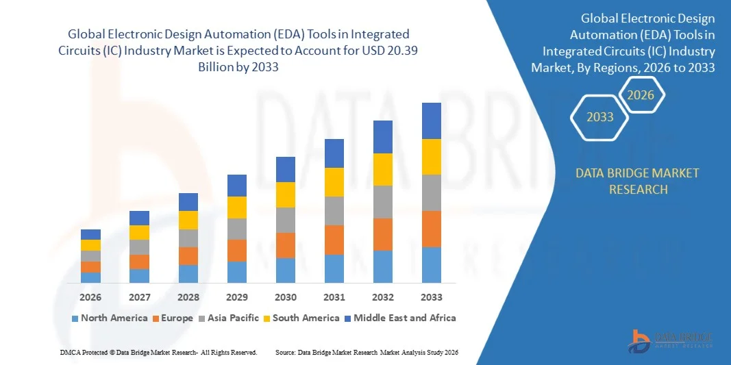
- The global electronic design automation (EDA) tools in integrated circuits (IC) industry market size was valued at USD 11.78 billion in 2025 and is expected to reach USD 20.39 billion by 2033, at a CAGR of 7.10% during the forecast period
- The market growth is largely fueled by the increasing complexity of semiconductor designs and the rapid advancement of technologies such as artificial intelligence, 5G, and high-performance computing, which require highly sophisticated Electronic Design Automation (EDA) tools to ensure accuracy, efficiency, and faster time-to-market
- Furthermore, rising demand for smaller, power-efficient, and high-performance integrated circuits across industries such as consumer electronics, automotive, and communication is establishing EDA tools as essential solutions for modern chip development. These converging factors are accelerating the adoption of advanced design and verification tools, thereby significantly boosting the industry's growth
Electronic Design Automation (EDA) Tools in Integrated Circuits (IC) Industry Market Analysis
- Electronic Design Automation (EDA) tools are software solutions used for designing, simulating, verifying, and manufacturing integrated circuits and electronic systems. These tools enable engineers to manage complex chip architectures, optimize performance, and reduce design errors while supporting advanced semiconductor fabrication processes
- The escalating demand for EDA tools is primarily fueled by the continuous evolution of semiconductor technologies, increasing integration of electronics in automotive and industrial applications, and the growing need for efficient and reliable chip design processes to support next-generation digital innovations
- North America dominated the Electronic Design Automation (EDA) Tools in Integrated Circuits (IC) Industry market with a share of around 40% in 2025, due to the strong presence of leading semiconductor companies and advanced chip design infrastructure across the region
- Asia-Pacific is expected to be the fastest growing region in the Electronic Design Automation (EDA) Tools in Integrated Circuits (IC) Industry market during the forecast period due to rapid expansion of semiconductor manufacturing and increasing investments in electronics production across countries such as China, Japan, South Korea, and India
- IC physical design and verification segment dominated the market with a market share of 39.1% in 2025, due to the increasing complexity of advanced node semiconductor designs and the critical need for accuracy in layout and validation processes. Chipmakers rely heavily on these tools to ensure performance, power efficiency, and manufacturability before fabrication, reducing costly design errors
Report Scope and Electronic Design Automation (EDA) Tools in Integrated Circuits (IC) Industry Market Segmentation
|
Attributes |
Electronic Design Automation (EDA) Tools in Integrated Circuits (IC) Industry Key Market Insights |
|
Segments Covered |
|
|
Countries Covered |
North America
Europe
Asia-Pacific
Middle East and Africa
South America
|
|
Key Market Players |
|
|
Market Opportunities |
|
|
Value Added Data Infosets |
In addition to the market insights such as market value, growth rate, market segments, geographical coverage, market players, and market scenario, the market report curated by the Data Bridge Market Research team includes in-depth expert analysis, import/export analysis, pricing analysis, production consumption analysis, and pestle analysis. |
Electronic Design Automation (EDA) Tools in Integrated Circuits (IC) Industry Market Trends
“Rising Adoption of AI-Driven Design Automation in Semiconductor Development”
- A significant trend in the Electronic Design Automation (EDA) Tools in Integrated Circuits (IC) market is the increasing adoption of artificial intelligence to automate complex chip design processes, driven by the need to manage rising design complexity and reduce development timelines across semiconductor industries. This integration is enhancing design accuracy, improving productivity, and enabling faster innovation in advanced semiconductor technologies
- For instance, Cadence Design Systems and Synopsys have introduced AI-powered EDA platforms such as Cadence Cerebrus and Synopsys DSO.ai that optimize chip design workflows and improve performance outcomes. These solutions enable engineers to explore design possibilities more efficiently and reduce time-to-market for next-generation chips
- The adoption of AI-driven tools is expanding in advanced node semiconductor development where traditional design approaches struggle to handle increasing transistor density and power constraints. This is positioning AI-enabled EDA tools as essential for achieving optimal performance and efficiency in modern chip architectures
- The growing use of AI in verification and simulation processes is enabling faster identification of design flaws and improving overall chip reliability. This trend is reducing costly errors and supporting higher success rates in semiconductor fabrication
- Industries focusing on high-performance computing, automotive electronics, and communication systems are increasingly integrating AI-based EDA tools to accelerate innovation and meet evolving performance requirements. This is shaping a stronger demand for intelligent automation across semiconductor design environments
- The market is witnessing continuous advancement in AI-driven design technologies that enhance scalability and adaptability in chip development processes. This rising adoption is reinforcing the transition toward more automated, efficient, and intelligent semiconductor design ecosystems globally
Electronic Design Automation (EDA) Tools in Integrated Circuits (IC) Industry Market Dynamics
Driver
“Increasing Complexity of Advanced Node Chip Design”
- The increasing complexity of advanced node semiconductor designs is driving the demand for highly sophisticated Electronic Design Automation (EDA) tools capable of managing intricate chip architectures and ensuring accurate design validation. These tools enable engineers to handle challenges related to power consumption, performance optimization, and manufacturability at smaller process nodes
- For instance, Intel’s development of its 18A process technology with RibbonFET and PowerVia architecture requires advanced EDA tools from companies such as Synopsys and Cadence to support design and verification processes. These technologies demand precise modeling and simulation capabilities to ensure successful chip production at nanoscale levels
- The rapid evolution of technologies such as artificial intelligence, 5G, and data centers is increasing the need for high-performance integrated circuits, further intensifying design complexity. This is boosting reliance on advanced EDA solutions that can support multi-layered and high-density chip designs
- The growing adoption of system-on-chip and heterogeneous integration approaches is adding further complexity to semiconductor development, requiring advanced tools for seamless integration and optimization. This is strengthening the role of EDA tools in modern chip design workflows
- The continuous increase in chip complexity and shrinking process nodes is reinforcing this driver, positioning EDA tools as indispensable for achieving high-performance, reliable, and scalable semiconductor solutions
Restraint/Challenge
“High Cost and Technical Complexity of Advanced EDA Solutions”
- The Electronic Design Automation (EDA) Tools in Integrated Circuits (IC) market faces challenges due to the high cost and technical complexity associated with advanced EDA platforms, which require significant investment in software licenses, infrastructure, and skilled professionals. These factors create barriers for small and mid-sized companies entering the semiconductor design space
- For instance, Siemens Digital Industries Software provides advanced EDA solutions such as Calibre for design verification, which require substantial financial and technical resources for implementation and operation. The complexity of these tools necessitates specialized expertise, increasing operational costs for organizations
- The integration of multiple EDA tools across design, verification, and simulation stages adds further complexity to semiconductor workflows, making it difficult for companies to streamline processes efficiently. This results in longer development cycles and increased dependency on skilled engineers
- The need for continuous updates and upgrades to keep pace with evolving semiconductor technologies further increases the total cost of ownership for EDA tools. Companies must invest regularly to maintain competitiveness and ensure compatibility with advanced process nodes
- The market continues to face constraints related to balancing high performance and cost efficiency, which may hinder adoption among smaller players. These challenges collectively impact the scalability and accessibility of advanced EDA solutions while maintaining the need for continuous innovation
Electronic Design Automation (EDA) Tools in Integrated Circuits (IC) Industry Market Scope
The market is segmented on the basis of type, component, deployment, end-user, and application.
• By Type
On the basis of type, the Electronic Design Automation (EDA) Tools in Integrated Circuits (IC) market is segmented into Computer-Aided Engineering (CAE), IC Physical Design and Verification, Printed Circuit Board and Multi-chip Module (PCB and MCM), and Semiconductor Intellectual Property (SIP). The IC Physical Design and Verification segment dominated the largest market revenue share of 39.1% in 2025, driven by the increasing complexity of advanced node semiconductor designs and the critical need for accuracy in layout and validation processes. Chipmakers rely heavily on these tools to ensure performance, power efficiency, and manufacturability before fabrication, reducing costly design errors. The rising adoption of AI-driven verification techniques and demand for high-performance computing chips further strengthens this segment’s leadership.
The Semiconductor Intellectual Property (SIP) segment is anticipated to witness the fastest growth rate from 2026 to 2033, fueled by the growing trend of reusable IP cores in chip design to accelerate time-to-market. Companies increasingly integrate pre-verified IP blocks for processors, memory, and interfaces, reducing design cycles and development costs. The expansion of IoT, 5G, and AI applications is further increasing demand for customizable and scalable IP solutions across semiconductor ecosystems.
• By Component
On the basis of component, the market is segmented into Solution and Services. The Solution segment dominated the largest market revenue share in 2025, driven by the extensive adoption of advanced EDA software platforms for design, verification, and simulation tasks. These solutions form the backbone of semiconductor development workflows, enabling engineers to handle complex chip architectures and multi-layer designs efficiently. Continuous innovation in software capabilities, including AI-assisted design automation and real-time analysis, supports the dominance of this segment.
The Services segment is expected to witness the fastest growth rate from 2026 to 2033, driven by the rising demand for consulting, customization, and support services to optimize EDA tool utilization. Semiconductor companies increasingly seek expert guidance for tool integration, workflow optimization, and training to manage complex design environments. The growing outsourcing of design services and the need for specialized expertise are accelerating the expansion of this segment.
• By Deployment
On the basis of deployment, the market is segmented into Cloud and On-Premise. The On-Premise segment dominated the largest market revenue share in 2025, driven by the need for high data security, control, and performance in semiconductor design processes. Large enterprises prefer on-premise deployment to safeguard sensitive intellectual property and maintain compliance with strict regulatory requirements. The requirement for high computational power and low latency in design simulations further supports the dominance of on-premise systems.
The Cloud segment is anticipated to witness the fastest growth rate from 2026 to 2033, fueled by increasing adoption of scalable and cost-effective computing resources for complex chip design tasks. Cloud-based EDA tools enable collaborative design, faster simulation, and reduced infrastructure costs, making them attractive for startups and mid-sized firms. The growing availability of secure cloud environments and integration with AI-driven workflows is further accelerating adoption.
• By End-user
On the basis of end-user, the market is segmented into Communication, Consumer Electronics, Computer, Automotive, Industrial, and Others. The Consumer Electronics segment dominated the largest market revenue share in 2025, driven by the high demand for advanced chips used in smartphones, wearables, and smart home devices. Continuous innovation in compact and power-efficient semiconductor components for consumer applications drives extensive use of EDA tools in this segment. Rapid product cycles and increasing feature integration further strengthen its leading position.
The Automotive segment is expected to witness the fastest growth rate from 2026 to 2033, fueled by the increasing integration of electronics in vehicles, including ADAS, electric powertrains, and infotainment systems. The shift toward autonomous driving and connected vehicles is significantly raising the demand for sophisticated chip designs. This trend is driving higher adoption of EDA tools for ensuring safety, reliability, and performance in automotive semiconductor development.
• By Application
On the basis of application, the market is segmented into Design, Verification, and Simulation. The Design segment dominated the largest market revenue share in 2025, driven by the growing complexity of integrated circuit architectures and the need for efficient layout and synthesis tools. Designers rely heavily on advanced EDA solutions to optimize chip performance, reduce power consumption, and manage increasing transistor densities. Continuous advancements in design automation technologies further support this segment’s leadership.
The Verification segment is anticipated to witness the fastest growth rate from 2026 to 2033, fueled by the rising need to detect and eliminate design flaws before fabrication. Increasing chip complexity and shrinking node sizes make verification a critical and resource-intensive stage in semiconductor development. The adoption of AI-driven verification tools and formal verification methods is accelerating growth, ensuring higher reliability and reducing costly post-production errors.
Electronic Design Automation (EDA) Tools in Integrated Circuits (IC) Industry Market Regional Analysis
- North America dominated the Electronic Design Automation (EDA) Tools in Integrated Circuits (IC) Industry market with the largest revenue share of around 40% in 2025, driven by the strong presence of leading semiconductor companies and advanced chip design infrastructure across the region
- Companies in the region highly prioritize innovation, high-performance computing, and advanced node semiconductor development, which significantly drives the adoption of sophisticated EDA tools
- This widespread adoption is further supported by substantial R&D investments, a mature semiconductor ecosystem, and increasing demand for AI, 5G, and data center technologies, establishing EDA tools as critical solutions for chip design and verification across industries
U.S. Electronic Design Automation (EDA) Tools in Integrated Circuits (IC) Market Insight
The U.S. market captured the largest revenue share in 2025 within North America, fueled by the presence of major semiconductor firms and continuous advancements in chip design technologies. Companies are increasingly investing in cutting-edge EDA tools to support the development of high-performance processors and AI-driven applications. The growing focus on innovation, coupled with strong collaboration between technology firms and research institutions, further accelerates market growth. Moreover, increasing demand for cloud computing, automotive electronics, and advanced communication systems is significantly contributing to the expansion of the EDA tools industry.
Europe Electronic Design Automation (EDA) Tools in Integrated Circuits (IC) Market Insight
The Europe market is projected to expand at a substantial CAGR throughout the forecast period, primarily driven by the growing emphasis on automotive electronics and industrial automation. The increasing adoption of advanced semiconductor technologies in electric vehicles and smart manufacturing is fostering demand for EDA tools. European companies are also focusing on energy-efficient and sustainable chip designs, further boosting tool adoption. The region is witnessing steady growth across automotive, industrial, and communication sectors, with EDA tools playing a crucial role in innovation and compliance with regulatory standards.
U.K. Electronic Design Automation (EDA) Tools in Integrated Circuits (IC) Market Insight
The U.K. market is anticipated to grow at a noteworthy CAGR during the forecast period, driven by rising investments in semiconductor research and development and increasing demand for advanced electronics. The country’s focus on innovation in AI, telecommunications, and chip design is encouraging the adoption of EDA tools. In addition, strong academic and research collaborations are supporting advancements in integrated circuit design. The expanding presence of technology startups and design firms is expected to continue stimulating market growth.
Germany Electronic Design Automation (EDA) Tools in Integrated Circuits (IC) Market Insight
The Germany market is expected to expand at a considerable CAGR during the forecast period, fueled by strong demand for semiconductor solutions in automotive and industrial applications. Germany’s leadership in automotive engineering and Industry 4.0 initiatives promotes the adoption of advanced chip design tools. The increasing focus on electric vehicles and automation technologies further drives the need for efficient EDA solutions. Integration of advanced semiconductor technologies with industrial systems is also becoming increasingly prevalent, aligning with the country’s emphasis on precision and innovation.
Asia-Pacific Electronic Design Automation (EDA) Tools in Integrated Circuits (IC) Market Insight
The Asia-Pacific market is poised to grow at the fastest CAGR during the forecast period of 2026 to 2033, driven by rapid expansion of semiconductor manufacturing and increasing investments in electronics production across countries such as China, Japan, South Korea, and India. The region’s strong manufacturing base and growing demand for consumer electronics are accelerating the adoption of EDA tools. Furthermore, government initiatives supporting semiconductor self-sufficiency and digital transformation are boosting market growth. As APAC emerges as a global hub for semiconductor fabrication, the demand for advanced design and verification tools continues to rise.
Japan Electronic Design Automation (EDA) Tools in Integrated Circuits (IC) Market Insight
The Japan market is gaining momentum due to its advanced electronics industry, strong focus on innovation, and demand for high-quality semiconductor components. The country emphasizes precision engineering and efficient chip design, driving the adoption of EDA tools. Increasing integration of semiconductors in automotive and consumer electronics sectors is fueling growth. Moreover, Japan’s continuous investments in research and development are supporting advancements in next-generation semiconductor technologies.
China Electronic Design Automation (EDA) Tools in Integrated Circuits (IC) Market Insight
The China market accounted for the largest market revenue share in Asia Pacific in 2025, attributed to the country’s massive semiconductor manufacturing capacity and rapid technological advancements. China is heavily investing in domestic semiconductor development, increasing the demand for EDA tools. The expansion of consumer electronics, telecommunications, and data center industries is further driving market growth. The push toward self-reliance in semiconductor production, supported by government initiatives and local players, is a key factor propelling the adoption of EDA tools in the country.
Electronic Design Automation (EDA) Tools in Integrated Circuits (IC) Industry Market Share
The Electronic Design Automation (EDA) Tools in Integrated Circuits (IC) Industry is primarily led by well-established companies, including:
- Infochips (an Arrow Company) (U.S.)
- Altium Limited (U.S.)
- ANSYS, Inc. (U.S.)
- Cadence Design Systems, Inc. (U.S.)
- Agnisys, Inc. (U.S.)
- Aldec, Inc. (U.S.)
- Mentor (a Siemens Business) (U.S.)
- Siemens AG (Germany)
- Synopsys, Inc. (U.S.)
- Zuken Inc. (Japan)
- Sigasi (Belgium)
- National Instruments Corporation (U.S.)
- Intercept Technology Inc. (U.S.)
- Silvaco, Inc. (U.S.)
Latest Developments in Global Electronic Design Automation (EDA) Tools in Integrated Circuits (IC) Industry Market
- In June 2025, Siemens Digital Industries Software introduced Innovator 3D IC and Calibre 3D Stress, significantly strengthening the Electronic Design Automation (EDA) tools market by addressing complex challenges associated with 2.5D and 3D IC architectures, including thermal stress, signal integrity, and multi-die integration. These tools enhance simulation accuracy and enable designers to predict long-term reliability issues early in the design cycle, reducing costly post-fabrication failures. This advancement is accelerating the transition toward heterogeneous integration and chiplet-based designs, thereby increasing the reliance on advanced EDA solutions for next-generation semiconductor development
- In February 2025, Intel launched a dedicated platform for its 18A process technology featuring RibbonFET transistors and PowerVia, creating a strong impact on the EDA tools market by pushing the boundaries of advanced node semiconductor design. The introduction of such cutting-edge architectures requires highly sophisticated design, verification, and simulation tools capable of handling increased complexity and tighter tolerances. This development is driving semiconductor companies to upgrade their EDA capabilities, thereby boosting demand for tools that support nanoscale innovation and high-performance chip production
- In December 2024, Samsung Semiconductor India Research introduced the “Chip Design for High School” program, contributing to the long-term growth of the EDA tools market by building a foundational talent pipeline in semiconductor design. By exposing students at an early stage to chip design concepts, the initiative is expected to increase awareness and interest in EDA technologies, ultimately leading to a more skilled workforce. This strategic move supports the expansion of the semiconductor ecosystem, particularly in emerging markets, and ensures sustained demand for EDA tools in the future
- In November 2024, Keysight Technologies launched an AI- and machine learning-based EDA software suite, enhancing the market by enabling faster and more efficient design processes for complex RF and high-frequency devices. The integration of AI-driven capabilities allows engineers to automate repetitive tasks, optimize designs, and identify potential issues more quickly, significantly reducing development time and costs. This innovation is promoting the adoption of intelligent design workflows, thereby increasing productivity and strengthening the role of advanced EDA tools in modern semiconductor engineering
- In June 2024, Siemens Digital Industries Software collaborated with Intel Foundry to develop a new EDA certification focused on embedded multi-die interconnect bridge technology, positively influencing the market by establishing standardized design methodologies for advanced packaging solutions. This collaboration improves interoperability between tools and foundry processes, enabling more efficient development of multi-die systems. It also supports innovation in chip packaging technologies, which are critical for improving performance, scalability, and power efficiency, thereby driving further adoption of specialized EDA solutions
- Interactive Data Analysis Dashboard
- Company Analysis Dashboard for high growth potential opportunities
- Research Analyst Access for customization & queries
- Competitor Analysis with Interactive dashboard
- Latest News, Updates & Trend analysis
- Harness the Power of Benchmark Analysis for Comprehensive Competitor Tracking
Data collection and base year analysis are done using data collection modules with large sample sizes. The stage includes obtaining market information or related data through various sources and strategies. It includes examining and planning all the data acquired from the past in advance. It likewise envelops the examination of information inconsistencies seen across different information sources. The market data is analysed and estimated using market statistical and coherent models. Also, market share analysis and key trend analysis are the major success factors in the market report. To know more, please request an analyst call or drop down your inquiry.
The key research methodology used by DBMR research team is data triangulation which involves data mining, analysis of the impact of data variables on the market and primary (industry expert) validation. Data models include Vendor Positioning Grid, Market Time Line Analysis, Market Overview and Guide, Company Positioning Grid, Patent Analysis, Pricing Analysis, Company Market Share Analysis, Standards of Measurement, Global versus Regional and Vendor Share Analysis. To know more about the research methodology, drop in an inquiry to speak to our industry experts.
Data Bridge Market Research is a leader in advanced formative research. We take pride in servicing our existing and new customers with data and analysis that match and suits their goal. The report can be customized to include price trend analysis of target brands understanding the market for additional countries (ask for the list of countries), clinical trial results data, literature review, refurbished market and product base analysis. Market analysis of target competitors can be analyzed from technology-based analysis to market portfolio strategies. We can add as many competitors that you require data about in the format and data style you are looking for. Our team of analysts can also provide you data in crude raw excel files pivot tables (Fact book) or can assist you in creating presentations from the data sets available in the report.