

What is the Flip Chip Technology Market Size and Growth Rate?
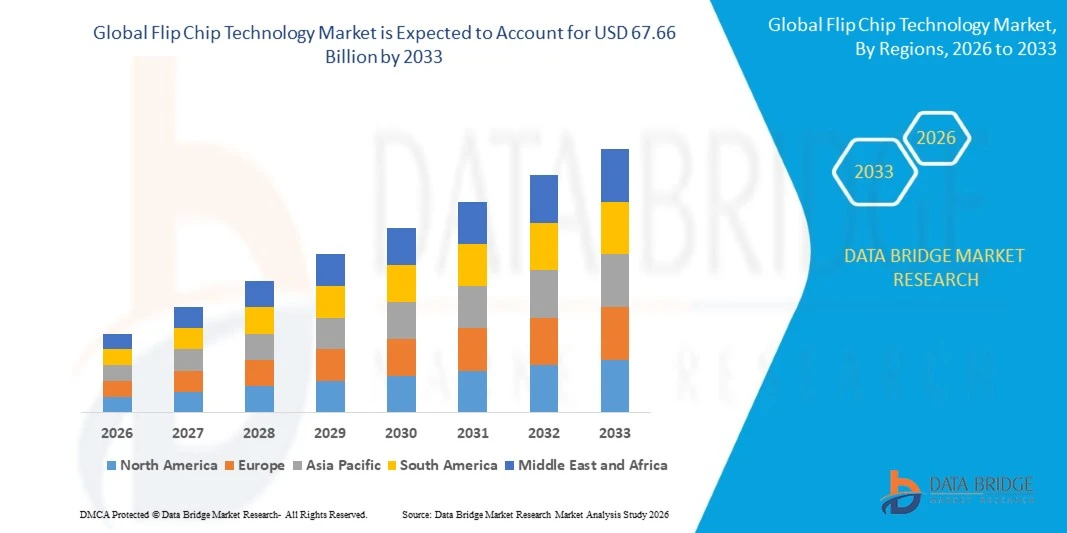
- As per Data Bridge Market Research analysis, the flip chip technology market was valued at USD 37.1 Billion in 2025 and is projected to reach USD 67.66 Billion by 2033, growing at a CAGR of 7.80% from 2026 to 2033.
- The market is benefiting from the semiconductor industry's broad transition toward chiplet-based architectures, which require dense, thermally efficient interconnects that flip chip packaging is well positioned to deliver across high-performance computing, AI, and mobile applications.
- Rising demand for GPUs and AI accelerators, along with continued growth in 5G infrastructure and high-bandwidth memory, is driving sustained investment in copper pillar and hybrid bonding interconnect technologies among IDMs, foundries, and OSATs.
Market Size & Forecast
- Global Market Value (2025): USD 37.1 Billion
- Expected Market Value (2033): USD 67.66 Billion
- Forecast CAGR (2026–2033): 7.80%
- Leading Region in 2025: Asia-Pacific
- Fastest Growing Region: North America
What are the Major Takeaways of the Flip Chip Technology Market?
- Asia-Pacific dominated the global flip chip technology market with the largest revenue share of 61.40% in 2025, supported by the concentration of foundry and OSAT capacity in Taiwan, South Korea, and China.
- North America is expected to be the fastest-growing region at a CAGR of 9.20% from 2026 to 2033, fueled by incentive-driven expansion of domestic advanced packaging capacity and rising AI accelerator production by U.S.-based chipmakers.
- Copper pillar held the leading share of 49.20% by wafer bumping process in 2025, reflecting its dominance in high-density interconnect applications spanning server processors, networking ASICs, and mobile application processors.
- Cu-to-Cu hybrid bonding is projected to be the fastest-growing bumping process segment, registering a CAGR of 10.30%, driven by accelerating adoption of sub-5 micron pitch requirements for next-generation high-bandwidth memory and logic-on-logic architectures.
- FC-BGA led the market with a 40.40% share by packaging technology in 2025, driven by server-class processor packaging demand from data center and AI infrastructure buildouts.
- Fan-Out wafer-level and panel-level packaging is expected to be the fastest-growing packaging technology segment, projected to grow at a CAGR of 10.70%, as cost-optimized heterogeneous integration reaches mid-tier applications.
- Memory devices accounted for 34.20% of the market by product in 2025, while GPU and AI accelerator packaging is expected to register the fastest growth among product segments, at a CAGR of 13.40%.
- Consumer electronics and wearables represented the leading end-use industry segment with a 31.10% share in 2025, while data-center and cloud applications are expected to see the fastest growth through the forecast period, at a CAGR of 8.56%.
Report Scope and Flip Chip Technology Market Segmentation
|
Attributes |
Flip Chip Technology Market Insights |
|
Segments Covered |
|
|
Countries Covered |
North America
Europe
Asia-Pacific
Middle East and Africa
South America
|
|
Key Market Players |
|
|
Market Opportunities |
|
|
Value Added Data Infosets |
In addition to the insights on market scenarios such as market value, growth rate, segmentation, geographical coverage, and major players, the market reports curated by the Data Bridge Market Research also include in-depth expert analysis, geographically represented company-wise production and capacity, network layouts of distributors and partners, detailed and updated price trend analysis and deficit analysis of supply chain and demand. |
What is the Key Trend in the Flip Chip Technology Market?
- Semiconductor manufacturers are accelerating adoption of Cu-to-Cu hybrid bonding to support sub-5 micron interconnect pitches required for next-generation high-bandwidth memory and logic-on-logic stacking.
- For instance, in 2025, a major networking equipment provider integrated flip chip packaged ASICs into its next-generation router line, achieving materially higher port throughput and lower operating temperatures compared with previous designs.
- Fan-out wafer-level and panel-level packaging are gaining traction as cost-optimized alternatives to traditional substrate-based flip chip packaging for mid-tier applications, expanding heterogeneous integration to a broader range of devices.
- For instance, in 2025, TSMC continued to scale its CoWoS advanced packaging capacity to meet surging demand for AI accelerator packaging, reflecting sustained capital investment in 2.5D interposer-based flip chip technology among leading foundries.
- OSATs and foundries are increasingly standardizing on panel-level packaging formats to improve manufacturing efficiency and lower per-unit costs as flip chip adoption extends into higher-volume, price-sensitive product categories.
- For instance, in 2025, ASE Technology Holding continued to expand its panel-level packaging pilot lines, targeting improved cost efficiency for fan-out based flip chip products serving mobile and consumer electronics customers.
- Growing use of copper pillar bumping in automotive power modules is extending flip chip technology beyond its traditional consumer and computing strongholds into higher-reliability industrial and transportation applications.
- For instance, in 2025, STMicroelectronics expanded its flip chip packaging capacity for automotive power management products, supporting rising demand from electric vehicle and ADAS customers.
- Overall, the flip chip technology market is moving toward higher-density interconnects, finer-pitch bumping, and advanced packaging architectures that support increasing computing performance while improving power efficiency and manufacturing economics. The growing adoption of hybrid bonding, copper pillar technology, fan-out wafer-level and panel-level packaging, and 2.5D/3D integration is expanding flip chip applications across AI, high-performance computing, automotive, communications, and consumer electronics.
What are the Key Drivers of the Flip Chip Technology Market?
- The rapid growth of AI accelerator and GPU demand is driving sustained investment in flip chip interconnect technologies capable of supporting the high pin counts and thermal loads required by high-performance computing packages.
- For instance, in 2025, Amkor Technology continued expansion of its advanced packaging facility in Arizona, adding flip chip and 2.5D packaging capacity to support U.S.-based customers in AI, high-performance computing, and automotive applications.
- Expanding 5G infrastructure deployment and growing automotive electronics content, particularly for ADAS and electric vehicle power management, are broadening flip chip adoption beyond traditional consumer electronics applications.
- For instance, in 2025, Samsung Electronics continued to expand its advanced packaging capacity to support flip chip-based memory and logic packaging for AI and mobile processor customers, reinforcing its position in the high-bandwidth memory supply chain.
- Rising demand for miniaturized, high-performance smartphones and wearables continues to support flip chip adoption, as the technology enables higher input/output density within increasingly compact form factors.
- For instance, in 2025, Texas Instruments expanded flip chip-based analog and power management IC production at its domestic fabrication facilities, supporting growing demand from industrial and automotive customers.
- Increasing outsourcing of advanced packaging by fabless semiconductor companies to specialized OSATs is expanding the addressable market for flip chip equipment and materials suppliers.
What Factors Are Challenging the Growth of the Flip Chip Technology Market?
- Flip chip packaging requires significant capital investment in bumping, underfill, and precision placement equipment, creating a high barrier to entry for smaller OSATs seeking to compete with established leaders.
- For instance, in 2025, several mid-tier OSATs cited the cost of qualifying Cu-to-Cu hybrid bonding equipment as a barrier to participating in next-generation high-bandwidth memory packaging, illustrating the capital intensity facing smaller providers relative to leading foundries.
- Ongoing geopolitical tensions and export-control measures affecting semiconductor equipment and materials continue to create supply-chain uncertainty for flip chip packaging capacity expansion in certain regions.
- Thermal management remains a persistent technical challenge as interconnect density rises, requiring continued innovation in underfill materials and heat-dissipation structures to prevent reliability issues in high-power packages.
- For instance, in 2025, several high-performance computing customers reported thermal-management-related qualification delays for next-generation flip chip packages with increased power density, highlighting the ongoing engineering challenge of managing heat in denser interconnect architectures.
- Overall, the growth of the flip chip technology market is being constrained by high capital requirements, increasing process complexity, supply-chain and geopolitical uncertainties, and thermal-management challenges associated with higher interconnect density and power consumption. These factors are increasing qualification requirements and manufacturing costs, particularly for smaller packaging providers, while encouraging continued investment in advanced materials, thermal solutions, process optimization, and equipment technologies.
How is the Flip Chip Technology Market Segmented?
The flip chip technology market is segmented on the basis of wafer bumping process, packaging technology, product, and end-use industry.
- By Wafer Bumping Process
On the basis of wafer bumping process, the market is segmented into copper pillar, tin-lead eutectic solder, lead-free solder/SAC, Cu-to-Cu hybrid bonding, and gold stud bump. Copper pillar held 49.2% revenue share in 2025, reflecting its dominance in high-density interconnect applications spanning server processors, networking ASICs, and mobile application processors.
Cu-to-Cu hybrid bonding is projected to be the fastest-growing segment, at a CAGR of 10.3% through the forecast period, as sub-5 micron pitch requirements accelerate adoption for next-generation high-bandwidth memory and logic-on-logic architectures.
- By Packaging Technology
On the basis of packaging technology, the market is segmented into FC-BGA, FCCSP/CSP, fan-out wafer-level/panel-level packaging, 2.5D interposer, and 3D stacked. FC-BGA led the market with a 40.4% share in 2025, driven by server-class processor packaging demand from data center and AI infrastructure buildouts.
Fan-out wafer-level and panel-level packaging are forecast to expand at a 10.7% CAGR, as cost-optimized heterogeneous integration reaches mid-tier consumer and industrial applications.
- By Product
On the basis of product, the market is segmented into memory (DRAM/NAND/HBM), CMOS image sensor, CPU/MPU, GPU/AI accelerator, networking/switch ASIC, and PMIC/analog. Memory devices accounted for 34.2% of 2025 revenue, supported by rising high-bandwidth memory content in AI and high-performance computing packages.
GPU and AI accelerator packaging is set to advance at a 13.4% CAGR, the fastest among product segments, driven by surging demand for AI training and inference infrastructure.
- By End-Use Industry
On the basis of end-use industry, the market is segmented into consumer electronics & wearables, data-center & cloud, automotive & transportation, industrial & robotics, telecommunications, and aerospace & defense. Consumer electronics and wearables held a 31.1% share in 2025, supported by continued flip chip adoption in smartphones, wearables, and compact consumer devices.
Data-center and cloud applications are expected to register an 8.56% CAGR through the forecast period, driven by continued AI infrastructure buildout and high-performance computing demand.
Which Region Holds the Largest Share of the Flip Chip Technology Market?
- Asia-Pacific dominated the global flip chip technology market and accounted for the largest revenue share of 61.40% in 2025, supported by the concentration of foundry and OSAT capacity in Taiwan, South Korea, and China, and sustained capital investment by leading semiconductor manufacturers.
- The region also benefits from established supply chains for substrates, bumping materials, and packaging equipment, along with continued government support for domestic advanced packaging capacity across multiple Asia-Pacific economies. Continued CoWoS and hybrid bonding capacity expansion by leading Taiwanese foundries is further reinforcing the region's leadership position.
U.K. Flip Chip Technology Market Insight
The U.K. flip chip technology market is supported by the country’s established semiconductor research ecosystem, growing investment in advanced packaging, and increasing demand for high-performance electronic components. Adoption of flip chip packaging is supported by applications in telecommunications, automotive electronics, aerospace, and high-performance computing, where compact form factors, improved electrical performance, and efficient thermal management are important. Furthermore, developments in heterogeneous integration, chiplet architectures, and advanced interconnect technologies are supporting demand for sophisticated flip chip solutions in the U.K.
Germany Flip Chip Technology Market Insight
The Germany flip chip technology market is expanding due to the country’s strong semiconductor, automotive, industrial electronics, and power electronics industries. Increasing adoption of advanced packaging for automotive processors, sensors, power management devices, and high-performance electronic systems is supporting demand for flip chip technologies. In addition, Germany’s focus on semiconductor manufacturing expansion, miniaturization, reliability, and advanced packaging research is encouraging the adoption of copper pillar, wafer-level packaging, and other high-density interconnect technologies.
Asia-Pacific Flip Chip Technology Market Insight
The Asia-Pacific flip chip technology market is witnessing strong growth, driven by the region’s concentration of semiconductor foundries, OSATs, electronics manufacturers, and advanced packaging facilities across Taiwan, China, South Korea, and Japan. Increasing demand for AI accelerators, high-bandwidth memory, smartphones, consumer electronics, automotive semiconductors, and high-performance computing is accelerating the adoption of flip chip and 2.5D/3D packaging technologies. Furthermore, investments in fan-out wafer-level packaging, copper pillar bumping, hybrid bonding, and heterogeneous integration are strengthening the regional flip chip ecosystem.
Japan Flip Chip Technology Market Insight
The Japan flip chip technology market is experiencing consistent growth, supported by the country’s advanced semiconductor materials and equipment industry, automotive electronics sector, and strong capabilities in precision manufacturing. Semiconductor manufacturers are increasingly adopting flip chip packaging for processors, memory devices, sensors, automotive electronics, and high-performance applications requiring compact designs and high electrical performance. Moreover, increasing investment in advanced packaging, chiplet integration, wafer-level packaging, and high-density interconnect technologies is supporting the development of next-generation flip chip solutions in Japan.
China Flip Chip Technology Market Insight
The China flip chip technology market is growing rapidly, supported by expanding domestic semiconductor manufacturing, increasing OSAT capacity, and government-backed efforts to strengthen the local semiconductor supply chain. Rising demand for smartphones, consumer electronics, automotive electronics, AI processors, and communications equipment is increasing the use of flip chip packaging across a broad range of semiconductor applications. In addition, investments in advanced packaging facilities, copper pillar bumping, fan-out packaging, and heterogeneous integration are strengthening domestic flip chip capabilities and supporting the transition toward higher-density semiconductor packaging.
Which are the Top Companies in Flip Chip Technology Market?
The flip chip technology industry is primarily led by well-established companies, including:
- Taiwan Semiconductor Manufacturing Company Limited (Taiwan)
- Intel Corporation (U.S.)
- Samsung Electronics Co., Ltd. (South Korea)
- Amkor Technology, Inc. (U.S.)
- ASE Technology Holding Co., Ltd. (Taiwan)
- Texas Instruments Incorporated (U.S.)
- United Microelectronics Corporation (Taiwan)
- STMicroelectronics N.V. (Switzerland)
- Powertech Technology Inc. (Taiwan)
- Jiangsu Changjiang Electronics Technology Co., Ltd. (China)
- 3M Company (U.S.)
- Fujitsu Limited (Japan)
- Advanced Semiconductor Engineering, Inc. (ASE) (Taiwan)
- JCET Group Co., Ltd. (China)
- Tongfu Microelectronics Co., Ltd. (China)
- Hana Micron Inc. (South Korea)
- Nepes Corporation (South Korea)
- Amkor Technology Korea, Inc. (South Korea)
- KYOCERA Corporation (Japan)
- ROHM Co., Ltd. (Japan)
- Renesas Electronics Corporation (Japan)
- Infineon Technologies AG (Germany)
- NXP Semiconductors N.V. (Netherlands)
- onsemi (U.S.)
- Broadcom Inc. (U.S.)
What are Latest Developments in Flip Chip Technology Market?
- In January 2025, TSMC reported continued investment in advanced packaging capacity as AI-related demand remained strong. The company maintained a 2025 capital expenditure plan of USD 38–42 billion, supporting advanced technology and packaging capacity. TSMC’s CoWoS platform integrates logic dies and high-bandwidth memory through advanced interposer-based packaging, reinforcing the role of flip-chip and related bump-based technologies in AI and high-performance computing applications.
- In April 2025, TSMC introduced additional advanced packaging developments for AI and high-performance computing at its North America Technology Symposium. The company announced continued expansion of its CoWoS roadmap, including plans for a 9.5-reticle-size CoWoS package capable of integrating 12 or more HBM stacks, with volume production targeted for 2027. TSMC also reported progress in advanced chip-stacking and interconnect technologies supporting increasingly complex AI processors.
- In April 2025, Amkor Technology entered into a strategic partnership with Intel to expand EMIB advanced-packaging assembly capacity across Korea, Portugal, and the United States. The collaboration is intended to increase availability of high-density multi-die packaging for AI, high-performance computing, and data-intensive applications. Although EMIB is a bridge-based technology rather than conventional flip chip, the development demonstrates the industry's broader movement toward high-density die-to-die interconnect and advanced packaging.
- In April 2025, Amkor highlighted increasing demand for 2.5D and RDL-based advanced packaging from high-performance computing and AI customers. During its first-quarter 2025 earnings discussion, the company reported continued engagement in 2.5D and RDL technologies and announced plans to expand its U.S. advanced-packaging footprint, with construction of its Arizona facility scheduled to begin in the second half of 2025.
- In February 2025, ASE officially launched its fifth plant in Penang, Malaysia, expanding the company's advanced packaging and testing footprint. The expansion increased the Malaysia site's planned floor space from approximately 1 million square feet to 3.4 million square feet and was driven partly by increasing demand for next-generation applications such as generative AI. ASE also maintains dedicated flip-chip packaging capabilities, including FCBGA and FCCSP technologies, supporting computing, telecommunications, memory, and other high-performance applications.
- In May 2025, TSMC approved approximately USD 15.25 billion in capital appropriations for capacity expansion, including advanced packaging, mature/specialty technologies, and fab construction. The investment formed part of TSMC's capacity planning based on market demand and its technology roadmap, supporting the continued scaling of advanced packaging infrastructure used in AI, HPC, and other high-performance semiconductor applications.
- In October 2025, Amkor broke ground on its advanced packaging and test campus in Arizona and increased the planned investment to USD 7 billion. The two-phase project is designed to provide more than 750,000 square feet of cleanroom space and support high-volume advanced packaging for AI, high-performance computing, mobile communications, and automotive applications. The facility is expected to begin production in early 2028 and represents a significant expansion of U.S.-based advanced packaging capacity.
- In 2025, TSMC reported that fine-pitch copper-bump technology for flip-chip packaging on its 2nm process successfully entered volume production. The development is particularly relevant to the flip chip technology market because copper-bump interconnects provide high-density electrical connections between the die and package while supporting increasingly advanced semiconductor process nodes. TSMC also reported that its CoWoS-L advanced packaging technology entered its second year of volume production in 2025.
- Interactive Data Analysis Dashboard
- Company Analysis Dashboard for high growth potential opportunities
- Research Analyst Access for customization & queries
- Competitor Analysis with Interactive dashboard
- Latest News, Updates & Trend analysis
- Harness the Power of Benchmark Analysis for Comprehensive Competitor Tracking
Global Flip Chip Technology Market, Supply Chain Analysis and Ecosystem Framework
To support market growth and help clients navigate the impact of geopolitical shifts, DBMR has integrated in-depth supply chain analysis into its Global Flip Chip Technology Market research reports. This addition empowers clients to respond effectively to global changes affecting their industries. The supply chain analysis section includes detailed insights such as Global Flip Chip Technology Market consumption and production by country, price trend analysis, the impact of tariffs and geopolitical developments, and import and export trends by country and HSN code. It also highlights major suppliers with data on production capacity and company profiles, as well as key importers and exporters. In addition to research, DBMR offers specialized supply chain consulting services backed by over a decade of experience, providing solutions like supplier discovery, supplier risk assessment, price trend analysis, impact evaluation of inflation and trade route changes, and comprehensive market trend analysis.
Data collection and base year analysis are done using data collection modules with large sample sizes. The stage includes obtaining market information or related data through various sources and strategies. It includes examining and planning all the data acquired from the past in advance. It likewise envelops the examination of information inconsistencies seen across different information sources. The market data is analysed and estimated using market statistical and coherent models. Also, market share analysis and key trend analysis are the major success factors in the market report. To know more, please request an analyst call or drop down your inquiry.
The key research methodology used by DBMR research team is data triangulation which involves data mining, analysis of the impact of data variables on the market and primary (industry expert) validation. Data models include Vendor Positioning Grid, Market Time Line Analysis, Market Overview and Guide, Company Positioning Grid, Patent Analysis, Pricing Analysis, Company Market Share Analysis, Standards of Measurement, Global versus Regional and Vendor Share Analysis. To know more about the research methodology, drop in an inquiry to speak to our industry experts.
Data Bridge Market Research is a leader in advanced formative research. We take pride in servicing our existing and new customers with data and analysis that match and suits their goal. The report can be customized to include price trend analysis of target brands understanding the market for additional countries (ask for the list of countries), clinical trial results data, literature review, refurbished market and product base analysis. Market analysis of target competitors can be analyzed from technology-based analysis to market portfolio strategies. We can add as many competitors that you require data about in the format and data style you are looking for. Our team of analysts can also provide you data in crude raw excel files pivot tables (Fact book) or can assist you in creating presentations from the data sets available in the report.