
Global Optical Lithography Market
Market Size in USD Billion
 USD
9.12 Billion
USD
14.32 Billion
2024
2032
USD
9.12 Billion
USD
14.32 Billion
2024
2032
| 2025 - 2032 | |
| USD 9.12 Billion | |
| USD 14.32 Billion | |
| % | |
Optical Lithography Market Analysis
The global optical lithography market is primarily driven by the increasing demand for miniaturized electronic devices and advanced semiconductor manufacturing technologies. Optical lithography is a critical process in semiconductor fabrication, enabling precise pattern transfer onto silicon wafers. As industries push toward smaller nodes and higher circuit densities, innovations such as extreme ultraviolet (EUV) lithography are transforming the market landscape. The adoption of optical lithography extends beyond semiconductors to other applications, including micro-electromechanical systems (MEMS), light-emitting diodes (LEDs), and photonics. Additionally, the rising demand for advanced displays and photonics in consumer electronics and automotive sectors is further fueling market growth.
Optical Lithography Market Size
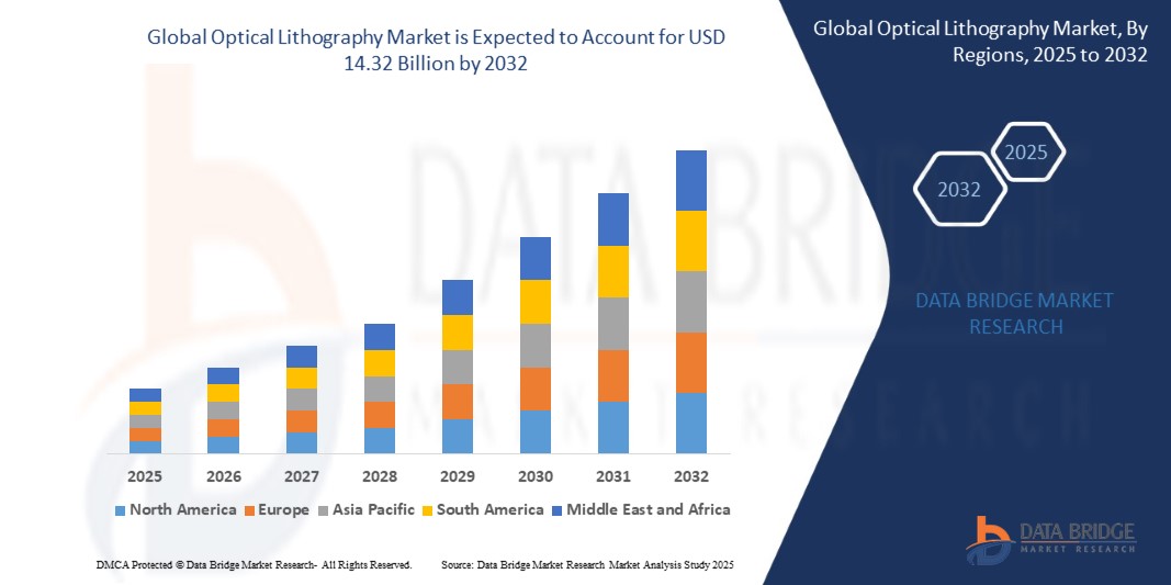
The global optical lithography market was valued at USD 9.12 billion in 2024 and is projected to reach USD 14.32 billion by 2032, growing at a CAGR of 5.8% during the forecast period of 2025 to 2032. In addition to the insights on market scenarios such as market value, growth rate, segmentation, geographical coverage, and major players, the market reports curated by the Data Bridge Market Research also include in-depth expert analysis, geographically represented company-wise production and capacity, network layouts of distributors and partners, detailed and updated price trend analysis and deficit analysis of supply chain and demand.
Optical Lithography Trends
“Demand for high-resolution patterning in consumer”
The optical lithography market is witnessing advancements in extreme ultraviolet (EUV) and ArF immersion technologies, enabling the production of sub-10nm semiconductor nodes. Demand for high-resolution patterning in consumer electronics and automotive industries is driving innovation. Additionally, increased investments in R&D by leading players are accelerating the adoption of photonics and advanced packaging solutions. Hybrid optical systems integrating machine learning are gaining popularity for enhanced precision. The market is also experiencing regional growth, particularly in Asia-Pacific, due to the proliferation of semiconductor manufacturing facilities.
Report Scope and Optical Lithography Market Segmentation
|
Attributes |
Optical Lithography Key Market Insights |
|
Segments Covered |
|
|
Countries Covered |
U.S., Canada, Mexico, Germany, France, U.K., Netherlands, Switzerland, Belgium, Russia, Italy, Spain, Turkey, Rest of Europe, China, Japan, India, South Korea, Singapore, Malaysia, Australia, Thailand, Indonesia, Philippines, Rest of Asia-Pacific, Saudi Arabia, U.A.E., South Africa, Egypt, Israel, Rest of Middle East and Africa, Brazil, Argentina, Rest of South America |
|
Key Market Players |
ASML Holding N.V. (Netherlands), Nikon Corporation (Japan), Canon Inc. (Japan), Ultratech (U.S.), SUSS MicroTec SE (Germany), Veeco Instruments Inc. (U.S.), KLA Corporation (U.S.), Lam Research Corporation (U.S.), Applied Materials Inc. (U.S.) |
|
Market Opportunities |
|
|
Value Added Data Infosets |
In addition to the insights on market scenarios such as market value, growth rate, segmentation, geographical coverage, and major players, the market reports curated by the Data Bridge Market Research also include in-depth expert analysis, geographically represented company-wise production and capacity, network layouts of distributors and partners, detailed and updated price trend analysis and deficit analysis of supply chain and demand. |
Optical Lithography Market Definition
The optical lithography market encompasses technologies used to transfer intricate patterns onto semiconductor wafers through light-based processes. This technique is integral to the fabrication of integrated circuits and advanced microchips, supporting industries such as electronics, automotive, and telecommunications. Optical lithography technologies, including ArF immersion and i-line, enable high-resolution patterning and are critical for producing sub-10nm semiconductor nodes. The market is driven by the growing demand for miniaturized devices, advanced packaging solutions, and photonics applications.
Optical Lithography Market Dynamics
Drivers
- Advancements in ArF Immersion Lithography.
ArF immersion lithography continues to be a critical driver as it bridges the gap between traditional optical lithography and EUV technologies. Its ability to produce highly precise patterns for sub-20nm nodes is essential for advanced semiconductor manufacturing. The growing demand for high-density memory chips and processors further propels adoption. With ongoing innovations, ArF immersion systems are achieving better throughput, enhancing production efficiency. This technology is particularly prominent in Asia-Pacific, where semiconductor foundries are expanding rapidly.
- Increasing Demand for Advanced Packaging
Advanced packaging techniques such as wafer-level packaging and 3D stacking are driving optical lithography adoption. These techniques require highly precise patterning to support complex chip designs, which optical lithography systems provide effectively. As industries such as automotive and AI demand smaller, faster, and more efficient devices, the role of optical lithography becomes increasingly vital. Additionally, the shift toward system-in-package (SiP) solutions further bolsters the technology’s importance. This trend is especially significant in consumer electronics, where innovation cycles are accelerating.
Opportunities
- Growth in Photonics Applications
The expanding photonics market, driven by demand for advanced optical components such as waveguides and photonic integrated circuits, offers significant opportunities. Optical lithography enables the creation of nanoscale features essential for these components, improving their performance. Applications in telecommunications, AR/VR, and medical imaging are fueling this growth. Increasing investments in R&D for photonics in regions such as Europe and North America amplify the market potential. As photonic technologies evolve, optical lithography’s role in their development becomes more integral.
- Proliferation of Semiconductor Foundries in Asia-Pacific
Asia-Pacific is emerging as a key region due to its rapidly growing semiconductor manufacturing infrastructure. Countries such as China, Taiwan, and South Korea are heavily investing in advanced lithography systems to enhance production capabilities. Government incentives and strategic partnerships between equipment manufacturers and foundries are accelerating adoption. The region’s focus on developing cutting-edge technologies, such as AI and IoT, drives demand for high-precision patterning solutions. This creates a substantial opportunity for optical lithography providers to expand their footprint.
Restraints/Challenges
- High Costs of Equipment Upgrades
Upgrading to advanced optical lithography systems, such as EUV, requires substantial investment, posing a significant challenge. Many manufacturers, especially smaller players, struggle to justify the capital expenditure amidst economic uncertainties. The cost of ancillary components, including masks and maintenance, further adds to the financial burden. Additionally, the lengthy implementation time for integrating these systems into production lines disrupts operations. This challenge is particularly evident in emerging economies, where cost sensitivity is higher.
- Limited Scalability Beyond EUV
The scalability of optical lithography beyond the EUV range is a limiting factor for future advancements. While EUV systems are effective for sub-7nm nodes, further scaling faces technical challenges such as photon shot noise and mask defects. These issues hinder the production of smaller and more complex nodes required for next-generation applications. The high costs and technical expertise needed for operating EUV systems exacerbate this restraint. Consequently, manufacturers are exploring alternative techniques such as nanoimprint lithography.
This market report provides details of new recent developments, trade regulations, import-export analysis, production analysis, value chain optimization, market share, impact of domestic and localized market players, analyses opportunities in terms of emerging revenue pockets, changes in market regulations, strategic market growth analysis, market size, category market growths, application niches and dominance, product approvals, product launches, geographic expansions, technological innovations in the market. To gain more info on the market contact Data Bridge Market Research for an Analyst Brief, our team will help you take an informed market decision to achieve market growth.
Global Optical Lithography Market Scope
The market is segmented into three notable segments based on technology, application, and end-use industry. The growth amongst these segments will help you analyze meagre growth segments in the industries and provide the users with a valuable market overview and market insights to help them make strategic decisions for identifying core market applications.
Technology
- i-Line
- KrF
- ArF Dry
- ArF Immersion
- EUV
Application
- Semiconductors
- MEMS
- LED
- Photonics
- Displays
End-Use Industry
- Electronics
- Automotive
- IT & Telecom
- Healthcare
- Aerospace & Defense
- Others
Global Optical Lithography Market Regional Analysis
The market is analyzed and market size insights and trends are provided by country, technology, application and end-use industry as referenced above.
The countries covered in the market are U.S., Canada, Mexico, Germany, France, U.K., Netherlands, Switzerland, Belgium, Russia, Italy, Spain, Turkey, rest of Europe, China, Japan, India, South Korea, Singapore, Malaysia, Australia, Thailand, Indonesia, Philippines, rest of Asia-Pacific, Saudi Arabia, U.A.E., South Africa, Egypt, Israel, rest of Middle East and Africa, Brazil, Argentina, and rest of South America.
North America is expected to dominate the optical lithography market due to its advanced semiconductor manufacturing capabilities and strong presence of key players such as Intel and GlobalFoundries. Robust R&D investments in photonics and advanced packaging technologies further bolster the region's leadership. Government initiatives to enhance domestic chip production, coupled with high demand for cutting-edge consumer electronics, drive growth. Additionally, collaborations between manufacturers and research institutions accelerate technological advancements in the region.
The country section of the report also provides individual market impacting factors and changes in regulation in the market domestically that impacts the current and future trends of the market. Data points such as down-stream and upstream value chain analysis, technical trends and porter's five forces analysis, case studies are some of the pointers used to forecast the market scenario for individual countries. Also, the presence and availability of global brands and their challenges faced due to large or scarce competition from local and domestic brands, impact of domestic tariffs and trade routes are considered while providing forecast analysis of the country data.
Global Optical Lithography Market Share
The market competitive landscape provides details by competitor. Details included are company overview, company financials, revenue generated, market potential, investment in research and development, new market initiatives, global presence, production sites and facilities, production capacities, company strengths and weaknesses, product launch, product width and breadth, application dominance. The above data points provided are only related to the companies' focus related to market.
Optical Lithography Market Leaders Operating in the Market Are:
- ASML Holding N.V. (Netherlands)
- Nikon Corporation (Japan)
- Canon Inc. (Japan)
- Ultratech (U.S.)
- SUSS MicroTec SE (Germany)
- Veeco Instruments Inc. (U.S.)
- KLA Corporation (U.S.)
- Lam Research Corporation (U.S.)
- Applied Materials Inc. (U.S.)
Latest Developments in Optical Lithography Market
- In 2020, Taiwan Semiconductor Manufacturing Co. (TSMC) announced that ~50% of all EUV lithography systems installed and operational worldwide are supplied by it. In November 2020, TSMC placed orders for 13 EUV systems with ASML. These systems are expected to be delivered throughout 2021, though the exact delivery and installation schedule is unknown. Meanwhile, the actual requirements of TSMC for the next year might be as high as 16–17 EUV scanners as the company is ramping-up production of chips using its fabrication technologies that feature EUV layers.
- In July 2020, Canon Inc. launched FPA-8000iW, the first Canon semiconductor lithography system to support manufacturing using large panels that are common in back-end processing.
SKU-
- Interactive Data Analysis Dashboard
- Company Analysis Dashboard for high growth potential opportunities
- Research Analyst Access for customization & queries
- Competitor Analysis with Interactive dashboard
- Latest News, Updates & Trend analysis
- Harness the Power of Benchmark Analysis for Comprehensive Competitor Tracking
Data collection and base year analysis are done using data collection modules with large sample sizes. The stage includes obtaining market information or related data through various sources and strategies. It includes examining and planning all the data acquired from the past in advance. It likewise envelops the examination of information inconsistencies seen across different information sources. The market data is analysed and estimated using market statistical and coherent models. Also, market share analysis and key trend analysis are the major success factors in the market report. To know more, please request an analyst call or drop down your inquiry.
The key research methodology used by DBMR research team is data triangulation which involves data mining, analysis of the impact of data variables on the market and primary (industry expert) validation. Data models include Vendor Positioning Grid, Market Time Line Analysis, Market Overview and Guide, Company Positioning Grid, Patent Analysis, Pricing Analysis, Company Market Share Analysis, Standards of Measurement, Global versus Regional and Vendor Share Analysis. To know more about the research methodology, drop in an inquiry to speak to our industry experts.
Data Bridge Market Research is a leader in advanced formative research. We take pride in servicing our existing and new customers with data and analysis that match and suits their goal. The report can be customized to include price trend analysis of target brands understanding the market for additional countries (ask for the list of countries), clinical trial results data, literature review, refurbished market and product base analysis. Market analysis of target competitors can be analyzed from technology-based analysis to market portfolio strategies. We can add as many competitors that you require data about in the format and data style you are looking for. Our team of analysts can also provide you data in crude raw excel files pivot tables (Fact book) or can assist you in creating presentations from the data sets available in the report.


