

What is the Semiconductor Metrology and Inspection Market Size and Growth Rate?
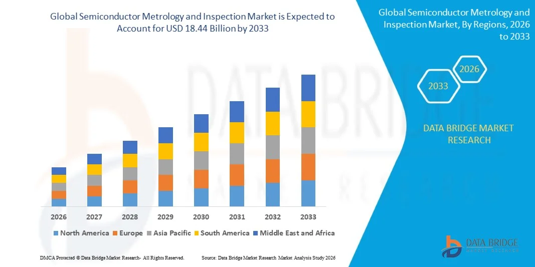
- As per Data Bridge Market Research analysis, the semiconductor metrology and inspection market was valued at USD 10.9 billion in 2025 and is projected to reach USD 18.44 billion by 2033, growing at a CAGR of 6.90% from 2026 to 2033.
- The market is experiencing consistent growth driven by the increasing adoption of advanced semiconductor manufacturing technologies, rising investments in semiconductor fabrication facilities, growing demand for high-precision process control, and the increasing need to detect defects and dimensional variations across increasingly complex semiconductor devices.
- The growing production of advanced semiconductor nodes, including 5 nm, 3 nm, and emerging sub-3 nm technologies, combined with increasing wafer complexity and the integration of advanced packaging technologies, is encouraging semiconductor manufacturers and foundries to strengthen metrology and inspection capabilities. Advanced inspection and metrology systems help identify defects at early production stages, improve yield, enhance process control, reduce manufacturing losses, and support the development of increasingly sophisticated semiconductor devices, contributing to the increasing demand for semiconductor metrology and inspection solutions globally.
Market Size & Forecast
- Global Market Value (2025): USD 10.9 Billion
- Expected Market Value (2033): USD 18.44 Billion
- Forecast CAGR (2026–2033): 6.90%
- Leading Region in 2025: North America
- Fastest Growing Region: Asia Pacific
What are the Major Takeaways of the Semiconductor Metrology and Inspection Market?
- Asia-Pacific dominated the semiconductor metrology and inspection market with the largest revenue share of 58.7% in 2025, supported by the strong concentration of semiconductor manufacturing capacity, expanding wafer fabrication facilities, and increasing investments in advanced semiconductor manufacturing technologies across China, Taiwan, South Korea, and Japan.
- North America is expected to be the fastest-growing region at a CAGR of 7.50% from 2026 to 2033, fueled by increasing investments in domestic semiconductor manufacturing, expansion of advanced fabrication facilities, growing adoption of advanced process-control technologies, and rising demand for high-precision metrology and inspection systems.
- The wafer inspection segment led the application category with a 44.3% share in 2025, driven by the increasing need to identify surface defects, pattern abnormalities, contamination, and other manufacturing irregularities during semiconductor wafer production.
- The lithography metrology segment is the fastest-growing application category, projected to register a CAGR of 8.00% from 2025 to 2030, reflecting increasing demand for precise overlay, critical-dimension, and pattern control as semiconductor manufacturers transition toward advanced process nodes.
- The optical segment dominated the type category with a 58.2% revenue share in 2025, supported by its high-speed, non-destructive measurement capabilities, broad application across semiconductor manufacturing processes, and suitability for inline process monitoring.
- The integrated circuit manufacturing segment led the application category with a 41.2% share in 2025, driven by increasing semiconductor production, continued development of advanced process nodes, and the growing requirement for precise defect detection, dimensional measurement, and process control.
- The foundries segment is the fastest-growing end-user category, projected to register a CAGR of 7.40% from 2026 to 2033, supported by expanding advanced-node fabrication capacity, increasing wafer production volumes, and growing adoption of metrology and inspection equipment for yield improvement and process optimization.
Report Scope and Semiconductor Metrology and Inspection Market Segmentation
|
Attributes |
Semiconductor Metrology and Inspection Key Market Insights |
|
Segments Covered |
|
|
Countries Covered |
North America
Europe
Asia-Pacific
Middle East and Africa
South America
|
|
Key Market Players |
|
|
Market Opportunities |
|
|
Value Added Data Infosets |
In addition to the insights on market scenarios such as market value, growth rate, segmentation, geographical coverage, and major players, the market reports curated by the Data Bridge Market Research also include in-depth expert analysis, geographically represented company-wise production and capacity, network layouts of distributors and partners, detailed and updated price trend analysis and deficit analysis of supply chain and demand. |
What is the Key Trend in the Semiconductor Metrology and Inspection Market?
- Semiconductor manufacturers and equipment suppliers are increasingly developing advanced metrology and inspection systems that combine optical inspection, e-beam inspection, defect review, and computational analysis to address the tighter process-control requirements of advanced logic, memory, and 3D semiconductor structures.
- For instance, in October 2025, Applied Materials introduced the PROVision 10 eBeam metrology system, designed to provide sub-nanometer resolution and faster throughput for complex 3D chips, supporting improved process control and yield in advanced semiconductor manufacturing.
- The increasing complexity of semiconductor architectures is driving greater adoption of e-beam metrology and inspection, particularly for detecting and characterizing nanoscale defects that are difficult to identify using optical inspection technologies.
- Semiconductor manufacturers are also expanding the use of advanced metrology and inspection technologies in high-bandwidth memory (HBM), chiplets, 2.5D and 3D architectures, and advanced packaging, where smaller features and increasingly complex structures require tighter process control.
- For instance, in June 2026, Applied Materials introduced new eBeam systems for advanced packaging, including the VeritySEM 7AP CD Metrology system, designed to measure features on thick, heterogeneous, and highly warped substrates used in HBM and chiplet architectures.
- As semiconductor manufacturing moves toward smaller process nodes, higher aspect-ratio structures, and increasingly complex 3D architectures, the development of high-resolution optical and e-beam metrology, automated defect classification, and integrated process-control solutions is expected to accelerate, reinforcing metrology and inspection as critical technologies for maintaining semiconductor yield and manufacturing quality.
What are the Key Drivers of the Semiconductor Metrology and Inspection Market?
- The rapid expansion of advanced semiconductor manufacturing, including GAA logic, DRAM, HBM, and advanced packaging, is increasing demand for high-precision metrology and inspection systems capable of controlling increasingly complex structures.
- For instance, in September 2025, Onto Innovation introduced the Atlas G6 OCD metrology system for advanced GAA and HBM production, addressing the need for improved measurement precision as device dimensions continue to shrink.
- Semiconductor manufacturers are increasingly integrating metrology and inspection with computational lithography and automated process-control systems to improve overlay accuracy, defect detection, process stability, and wafer yield.
- For instance, in September 2025, ASML showcased its holistic lithography portfolio at SEMICON India 2025, combining lithography systems, computational software, metrology, and inspection solutions to help semiconductor manufacturers improve process control, yield, and production performance.
- The expansion of advanced packaging, including 2.5D, 3D, and hybrid-bonding technologies, is also increasing the requirement for specialized metrology solutions capable of measuring increasingly complex semiconductor structures.
- For instance, in August 2025, Nova introduced the Nova WMC platform for advanced packaging, supporting multiple metrology technologies and wafer formats for applications including 2.5D and 3D packaging and hybrid bonding.
- With semiconductor manufacturers continuing to pursue smaller process geometries, higher transistor density, HBM architectures, and advanced packaging, increasing process complexity is driving greater reliance on metrology and inspection technologies to maintain dimensional accuracy, identify defects, and improve manufacturing yields.
Which Factors are Challenging the Growth of the Semiconductor Metrology and Inspection Market?
- Advanced semiconductor manufacturing introduces increasingly complex inspection and metrology requirements because smaller features, three-dimensional structures, and advanced packaging architectures require higher measurement sensitivity, resolution, and accuracy.
- For instance, in January 2025, the Government of the Netherlands announced expanded export-control requirements covering a limited range of advanced semiconductor manufacturing technologies, including certain measuring and inspection equipment used to identify wafer defects and improve measurement accuracy during chip production.
- These regulatory requirements can increase market complexity because manufacturers and equipment suppliers must account for licensing requirements and changing international controls when supplying advanced metrology and inspection technologies across different markets.
- The increasing complexity of semiconductor inspection also creates technical challenges because high-resolution inspection systems must balance defect sensitivity, measurement accuracy, inspection coverage, and throughput.
- For instance, ASML's 2025 Annual Report noted that e-beam inspection provides very high resolution but is traditionally slower than optical inspection, prompting the development of multibeam systems to increase inspection speed while maintaining high-resolution defect detection.
- In addition, the increasing volume of semiconductor inspection data creates challenges related to defect classification, analysis time, and automated decision-making, particularly as manufacturers seek to reduce manual intervention and accelerate yield learning.
How is the Semiconductor Metrology and Inspection Market Segmented?
The semiconductor metrology and inspection market is segmented on the basis of type, technology, dimension, application, and end use.
- By Type
On the basis of type, the semiconductor metrology and inspection market is segmented into optical and beam. The optical segment dominated the market with an estimated 64.5% share in 2025, supported by its high-speed inspection capability, broad process coverage, cost efficiency, and extensive deployment across semiconductor fabrication facilities. Optical systems are widely used for wafer inspection, critical dimension measurement, surface defect detection, overlay measurement, and process monitoring. Their ability to provide high-throughput, non-contact inspection makes them suitable for high-volume semiconductor manufacturing. Increasing semiconductor production and the transition toward advanced process nodes are further supporting demand for optical metrology and inspection systems. Advancements in optical imaging and automated defect analysis are also improving measurement accuracy and inspection efficiency.
The beam segment is projected to register the fastest growth at an estimated CAGR of 8.6% from 2026 to 2033, driven by increasing requirements for high-resolution inspection, nanoscale defect detection, and advanced semiconductor process control. Beam-based systems, particularly electron-beam inspection, provide detailed characterization capabilities for increasingly complex semiconductor structures. Their adoption is expanding across advanced logic, memory, EUV, and other leading-edge semiconductor manufacturing applications. Increasing device complexity and shrinking feature dimensions are creating greater requirements for high-resolution defect detection. Development of multibeam inspection technologies is also helping address throughput limitations associated with conventional beam-based systems. These developments are expected to accelerate adoption of beam inspection technologies.
- By Technology
On the basis of technology, the semiconductor metrology and inspection market is segmented into wafer inspection system, mask inspection system, thin film metrology, package inspection, and others. The wafer inspection system segment dominated the market with an estimated 44.7% share in 2025, supported by its essential role in detecting defects, contamination, pattern abnormalities, and process variations during semiconductor manufacturing. Wafer inspection systems enable manufacturers to identify defects at early stages of production and support yield improvement and process optimization. Increasing wafer fabrication capacity and shrinking semiconductor geometries are strengthening demand for high-sensitivity inspection systems. Manufacturers are also incorporating automated defect classification and advanced data analytics to improve inspection efficiency. The growing complexity of advanced logic and memory devices is further increasing the importance of wafer inspection systems.
The package inspection segment is projected to register the fastest growth at an estimated CAGR of 8.8% from 2026 to 2033, driven by increasing adoption of advanced packaging, chiplet architectures, heterogeneous integration, and 2.5D and 3D semiconductor packaging technologies. Package inspection systems are increasingly required to identify defects associated with bonding, alignment, interconnections, and package structures. The growing complexity of advanced semiconductor packages is increasing the need for high-resolution and automated inspection capabilities. Increasing investments in advanced packaging by semiconductor manufacturers and OSAT companies are also expanding demand for package inspection solutions. These developments are expected to accelerate adoption of package inspection technologies.
- By Dimension
On the basis of dimension, the semiconductor metrology and inspection market is segmented into 2D metrology/inspection, 3D metrology/inspection, and hybrid 2D/3D systems. The 2D metrology/inspection segment dominated the market with an estimated 57.4% share in 2025, supported by its widespread application in planar wafer inspection, critical dimension measurement, overlay control, and surface-level defect detection. Two-dimensional systems provide established and high-throughput measurement capabilities across semiconductor manufacturing processes. Their compatibility with existing process-control infrastructure supports broad adoption across mature and advanced manufacturing facilities. Increasing requirements for dimensional accuracy, defect detection, and process monitoring are supporting continued demand for 2D metrology and inspection systems.
The 3D metrology/inspection segment is projected to register the fastest growth at an estimated CAGR of 8.0% from 2026 to 2033, driven by increasing adoption of three-dimensional semiconductor structures, 3D NAND, advanced packaging, through-silicon vias, and stacked devices. Three-dimensional inspection provides enhanced measurement capabilities for structures that cannot be fully evaluated through conventional two-dimensional techniques. Increasing adoption of 2.5D and 3D packaging and complex device architectures is creating additional requirements for depth-sensitive and volumetric inspection. Manufacturers are also adopting 3D systems to improve structural characterization and identify defects within complex semiconductor architectures. These developments are expected to support rapid adoption of 3D metrology and inspection solutions.
- By Application
On the basis of application, the semiconductor metrology and inspection market is segmented into lithography metrology, wafer inspection, and thin film metrology. The wafer inspection segment dominated the market with an estimated 44.3% share in 2025, supported by its critical role in detecting defects, contamination, pattern variations, and other process abnormalities throughout semiconductor wafer manufacturing. Wafer inspection enables manufacturers to identify production defects and improve yield and process stability. Increasing semiconductor fabrication activity and the transition toward smaller process nodes are strengthening demand for advanced wafer inspection solutions. The integration of automated defect classification and data analytics is further improving inspection efficiency. Increasing complexity across logic and memory devices is expected to sustain demand for wafer inspection applications.
The lithography metrology segment is projected to register the fastest growth at an estimated CAGR of 8.0% from 2026 to 2033, driven by increasing requirements for overlay accuracy, critical dimension control, and precise pattern transfer at advanced semiconductor nodes. Lithography metrology enables manufacturers to monitor dimensional and alignment parameters that influence semiconductor yield and device performance. Increasing adoption of advanced lithography processes is creating additional requirements for high-precision metrology systems. Manufacturers are also integrating metrology with computational lithography and process-control platforms to improve manufacturing accuracy. These developments are expected to accelerate the adoption of lithography metrology across advanced semiconductor fabrication facilities.
- By End User
On the basis of end user, the semiconductor metrology and inspection market is segmented into semiconductor foundries, integrated device manufacturers (IDMs), outsourced semiconductor assembly and test (OSAT) companies, and research and development (R&D) institutions. The semiconductor foundries segment dominated the market with an estimated 52.8% share in 2025, supported by continuous investments in advanced logic manufacturing, high-volume wafer production, and leading-edge process node development. Foundries require metrology and inspection systems throughout wafer fabrication to maintain dimensional accuracy, identify defects, control process variations, and improve production yields. Increasing investments in AI processors, high-performance computing chips, advanced memory, and leading-edge semiconductor manufacturing are further strengthening demand from foundries. These factors are expected to sustain the segment's leading position.
The outsourced semiconductor assembly and test (OSAT) companies segment is projected to register the fastest growth at an estimated CAGR of 8.5% from 2026 to 2033, driven by increasing outsourcing of semiconductor assembly and testing, advanced packaging adoption, and growing demand for chiplet and heterogeneous integration technologies. OSAT companies increasingly require inspection and metrology systems to evaluate package integrity, bonding quality, alignment, interconnections, and structural characteristics. The adoption of 2.5D and 3D packaging is creating additional inspection requirements across assembly processes. Increasing investment in advanced packaging capacity is further supporting demand for specialized inspection technologies. These developments are expected to accelerate adoption of semiconductor metrology and inspection systems among OSAT companies.
Which Region Holds the Largest Share of the Semiconductor Metrology and Inspection Market?
- North America dominated the semiconductor metrology and inspection market with the largest revenue share of 38.5% in 2025, supported by the presence of leading semiconductor manufacturers, advanced fabrication facilities, established semiconductor equipment suppliers, and strong investments in process optimization and yield enhancement.
- The region also benefits from strong semiconductor research and development capabilities, growing investments in advanced fabrication capacity, and increasing adoption of high-precision metrology and inspection technologies. The expansion of advanced logic, memory, artificial intelligence, and high-performance computing semiconductor production is increasing demand for defect detection, critical dimension measurement, overlay control, and process monitoring solutions. The U.S. remains the major country-level market in North America, supported by semiconductor manufacturing investments and a strong equipment supplier ecosystem.
U.S. Semiconductor Metrology and Inspection Market Insight
The U.S. semiconductor metrology and inspection market is witnessing strong growth due to increasing investments in semiconductor manufacturing capacity, advanced process nodes, and next-generation chip architectures. The country benefits from the presence of major semiconductor equipment manufacturers and advanced semiconductor fabrication facilities, creating sustained demand for high-precision metrology and inspection systems. Increasing adoption of AI-enabled defect classification, inline inspection, and automated process control is further supporting market development. In addition, growing investments in artificial intelligence, high-performance computing, advanced logic, and memory semiconductor production are increasing requirements for accurate dimensional measurement, defect detection, and yield optimization.
Asia-Pacific Semiconductor Metrology and Inspection Market Insight
The Asia-Pacific semiconductor metrology and inspection market is expected to witness strong growth, driven by expanding semiconductor fabrication capacity, increasing advanced packaging activities, and rising investments in semiconductor manufacturing across China, Japan, South Korea, Taiwan, and other regional markets. The region benefits from a strong concentration of foundries, integrated device manufacturers, memory producers, and OSAT companies. Growing demand for AI semiconductors, consumer electronics, automotive chips, and advanced computing devices is increasing the need for wafer inspection, metrology, thin film measurement, and package inspection systems. Government-backed semiconductor development programs and supply-chain localization initiatives are further supporting regional market expansion.
Japan Semiconductor Metrology and Inspection Market Insight
The Japan semiconductor metrology and inspection market is witnessing consistent growth due to the country's established semiconductor equipment industry, precision-engineering capabilities, and advanced research and development infrastructure. Japanese semiconductor manufacturers and equipment suppliers are increasingly focusing on high-precision inspection, electron-beam technologies, optical metrology, and advanced process-control solutions. The presence of companies involved in semiconductor inspection and metrology equipment is supporting technological development and domestic demand. Increasing investments in advanced semiconductor manufacturing, memory technologies, and next-generation packaging are further creating opportunities for metrology and inspection systems.
China Semiconductor Metrology and Inspection Market Insight
The China semiconductor metrology and inspection market is growing due to expanding domestic semiconductor fabrication capacity, increasing efforts toward semiconductor supply-chain localization, and rising investments in advanced manufacturing infrastructure. The country has a large semiconductor manufacturing and electronics ecosystem, creating demand for wafer inspection, process metrology, and advanced packaging inspection technologies. Increasing development of domestic semiconductor manufacturing capabilities is supporting demand for process-control equipment. In addition, growing requirements for advanced logic, memory, power semiconductors, and packaging technologies are creating additional opportunities for high-precision metrology and inspection systems.
U.K. Semiconductor Metrology and Inspection Market Insight
The U.K. semiconductor metrology and inspection market is experiencing steady growth, supported by semiconductor research and development, advanced engineering capabilities, and increasing investment in semiconductor manufacturing and technology infrastructure. Research institutions and semiconductor companies are increasingly adopting precision measurement and inspection technologies for process development, device characterization, and quality control. Growing interest in compound semiconductors, advanced materials, photonics, and next-generation semiconductor technologies is creating additional requirements for metrology and inspection solutions. Furthermore, continued investment in semiconductor research and innovation is supporting demand for advanced measurement and inspection capabilities across research and production environments.
Germany Semiconductor Metrology and Inspection Market Insight
The Germany semiconductor metrology and inspection market is expanding steadily due to the country's strong industrial base, advanced engineering capabilities, and growing focus on semiconductor manufacturing for automotive, industrial, and power-electronics applications. Semiconductor manufacturers and technology companies are increasingly adopting advanced metrology and inspection systems to improve process control, defect detection, dimensional accuracy, and production quality. The country's automotive semiconductor ecosystem is also supporting demand for reliable inspection and quality-control technologies. Moreover, increasing investments in European semiconductor manufacturing capacity and advanced process technologies are creating additional opportunities for metrology and inspection equipment across Germany.
Which are the Top Companies in Semiconductor Metrology and Inspection Market?
The Semiconductor Metrology and Inspection industry is primarily led by well-established companies, including:
- KLA Corporation (U.S.)
- Applied Materials, Inc. (U.S.)
- ASML Holding N.V. (Netherlands)
- Onto Innovation Inc. (U.S.)
- Nova Ltd. (Israel)
- Hitachi High-Tech Corporation (Japan)
- JEOL Ltd. (Japan)
- Lasertec Corporation (Japan)
- Thermo Fisher Scientific Inc. (U.S.)
- Carl Zeiss AG (Germany)
- Camtek Ltd. (Israel)
- SCREEN Holdings Co., Ltd. (Japan)
- Nikon Corporation (Japan)
- Rigaku Corporation (Japan)
- Bruker Corporation (U.S.)
- Unity Semiconductor SAS (France)
- Toray Engineering Co., Ltd. (Japan)
- Confovis GmbH (Germany)
- Microtrac MRB (U.S.)
What are Latest Developments in Semiconductor Metrology and Inspection Market?
- In September 2025, Onto Innovation announced the launch of its Atlas G6 optical critical-dimension (OCD) metrology platform, designed to support process control for next-generation gate-all-around (GAA) logic and high-bandwidth memory (HBM) devices. The system incorporated a smaller measurement spot size, higher signal sensitivity, and enhanced precision to address increasingly complex semiconductor structures. Onto Innovation stated that the platform was developed to support structures shrinking by up to 30% per generation, highlighting the increasing importance of high-precision metrology for advanced semiconductor manufacturing.
- In August 2025, Nova announced the release of its Nova WMC next-generation modular optical metrology platform for advanced semiconductor packaging. The system was designed to support a wide range of wafer sizes and forms while incorporating multiple metrology technologies within a modular platform. The solution targets advanced 2.5D and 3D packaging applications and hybrid bonding processes, supporting increasing requirements for dimensional measurement and process control in advanced packaging manufacturing.
- In February 2025, Applied Materials introduced its SEMVision H20 defect review system, designed to improve the analysis of nanoscale defects in leading-edge semiconductor devices. The system combines high-resolution electron-beam imaging with AI-based image recognition to support faster defect detection and classification. The development addresses the increasing requirement to identify extremely small defects that can affect semiconductor performance as device geometries continue to shrink.
- In 2025, ASML highlighted the HMI eScan1100 multibeam inspection system as part of its semiconductor metrology and inspection portfolio. The system uses 25 electron beams to increase wafer coverage and inspection throughput, with ASML stating that it provides up to 10 times higher throughput than single-beam systems for advanced logic and DRAM applications. The development is intended to combine the high resolution of electron-beam inspection with higher throughput for advanced semiconductor process control and defect analysis.
- In January 2025, the Netherlands announced expanded export-control requirements covering a limited range of advanced semiconductor manufacturing technologies, including certain measuring and inspection equipment. The measures, which were scheduled to take effect from April 2025, included technologies used to detect defects in wafers and improve measurement precision following semiconductor processing steps. The development highlighted the increasing strategic importance of advanced metrology and inspection technologies within the global semiconductor manufacturing supply chain.
- Interactive Data Analysis Dashboard
- Company Analysis Dashboard for high growth potential opportunities
- Research Analyst Access for customization & queries
- Competitor Analysis with Interactive dashboard
- Latest News, Updates & Trend analysis
- Harness the Power of Benchmark Analysis for Comprehensive Competitor Tracking
Global Semiconductor Metrology And Inspection Market, Supply Chain Analysis and Ecosystem Framework
To support market growth and help clients navigate the impact of geopolitical shifts, DBMR has integrated in-depth supply chain analysis into its Global Semiconductor Metrology And Inspection Market research reports. This addition empowers clients to respond effectively to global changes affecting their industries. The supply chain analysis section includes detailed insights such as Global Semiconductor Metrology And Inspection Market consumption and production by country, price trend analysis, the impact of tariffs and geopolitical developments, and import and export trends by country and HSN code. It also highlights major suppliers with data on production capacity and company profiles, as well as key importers and exporters. In addition to research, DBMR offers specialized supply chain consulting services backed by over a decade of experience, providing solutions like supplier discovery, supplier risk assessment, price trend analysis, impact evaluation of inflation and trade route changes, and comprehensive market trend analysis.
Data collection and base year analysis are done using data collection modules with large sample sizes. The stage includes obtaining market information or related data through various sources and strategies. It includes examining and planning all the data acquired from the past in advance. It likewise envelops the examination of information inconsistencies seen across different information sources. The market data is analysed and estimated using market statistical and coherent models. Also, market share analysis and key trend analysis are the major success factors in the market report. To know more, please request an analyst call or drop down your inquiry.
The key research methodology used by DBMR research team is data triangulation which involves data mining, analysis of the impact of data variables on the market and primary (industry expert) validation. Data models include Vendor Positioning Grid, Market Time Line Analysis, Market Overview and Guide, Company Positioning Grid, Patent Analysis, Pricing Analysis, Company Market Share Analysis, Standards of Measurement, Global versus Regional and Vendor Share Analysis. To know more about the research methodology, drop in an inquiry to speak to our industry experts.
Data Bridge Market Research is a leader in advanced formative research. We take pride in servicing our existing and new customers with data and analysis that match and suits their goal. The report can be customized to include price trend analysis of target brands understanding the market for additional countries (ask for the list of countries), clinical trial results data, literature review, refurbished market and product base analysis. Market analysis of target competitors can be analyzed from technology-based analysis to market portfolio strategies. We can add as many competitors that you require data about in the format and data style you are looking for. Our team of analysts can also provide you data in crude raw excel files pivot tables (Fact book) or can assist you in creating presentations from the data sets available in the report.