
Global Semiconductor Wafer Cleaning Equipment Market
Market Size in USD Billion
 USD
9.30 Billion
USD
18.40 Billion
2024
2032
USD
9.30 Billion
USD
18.40 Billion
2024
2032
| 2025 - 2032 | |
| USD 9.30 Billion | |
| USD 18.40 Billion | |
| % | |
|
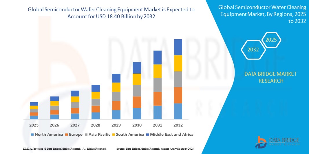
Semiconductor Wafer Cleaning Equipment Market Size
- The global Semiconductor Wafer Cleaning Equipment market size was valued at USD 9.3 billion in 2024 and is expected to reach USD 18.40 billion by 2032, at a CAGR of 8.9% during the forecast period
- The market growth is largely fuelled by the increasing demand for advanced electronic devices and the rapid expansion of the semiconductor industry. As chips become smaller and more powerful, maintaining wafer cleanliness becomes more critical to ensure performance and yield
- Furthermore, the rise in adoption of technologies like 5G, AI, and IoT is accelerating chip production, thereby boosting the need for efficient cleaning solutions. Additionally, the trend toward miniaturization in consumer electronics and automotive components is pushing manufacturers to adopt advanced wafer cleaning techniques. The surge in investments in semiconductor fabs, especially in Asia-Pacific and the U.S., is further fuelling market expansion.
Semiconductor Wafer Cleaning Equipment Market Analysis
- Semiconductor wafer cleaning equipment refers to the machinery that is utilized in semiconductor surface so that it can remove all the dust and other unwanted chemicals and particles without causing any harm to the surface.
- Tech cleaning technologies, front side up cleaning technology and wet chemistry based cleaning technology are some of the common technology which is used in the wafer cleaning equipment. These are widely used in application such as metallic contamination, particle contamination and chemical contamination.
- Asia-Pacific dominates the Semiconductor Wafer Cleaning Equipment market with the largest revenue share of 52.27% in 2025, characterized by increasing investments, business expansion capabilities for major key players, high presence of wafer, IC manufacturing firms, favorable economic conditions and cheap labor costs in the region.
- North America is expected to be the fastest growing region in the Semiconductor Wafer Cleaning Equipment market during the forecast period due to rise in the adoption of MEMS technology in patient monitoring devices to help revive the market during the COVID-19 pandemic and increase in the use of silicon-based sensors, chips, and diodes in IoT applications accelerate the market growth
- Wet Chemistry-Based Cleaning Technology segment is expected to dominate the Semiconductor Wafer Cleaning Equipment market with a market share of 56.11% in 2025, driven by its effectiveness in removing submicron particles and organic contaminants from complex wafer surfaces.
Report Scope and Semiconductor Wafer Cleaning Equipment Market Segmentation
|
Attributes |
Semiconductor Wafer Cleaning Equipment Key Market Insights |
|
Segments Covered |
|
|
Countries Covered |
North America
Europe
Asia-Pacific
Middle East and Africa
South America
|
|
Key Market Players |
|
|
Market Opportunities |
|
|
Value Added Data Infosets |
In addition to the insights on market scenarios such as market value, growth rate, segmentation, geographical coverage, and major players, the market reports curated by the Data Bridge Market Research also include in-depth expert analysis, pricing analysis, brand share analysis, consumer survey, demography analysis, supply chain analysis, value chain analysis, raw material/consumables overview, vendor selection criteria, PESTLE Analysis, Porter Analysis, and regulatory framework. |
Semiconductor Wafer Cleaning Equipment Market Trends
“Integration of Artificial Intelligence (AI) and Automation in Cleaning Systems”
- The semiconductor industry is increasingly adopting AI and automation technologies to enhance the efficiency and precision of wafer cleaning processes. AI-driven systems enable predictive maintenance, real-time monitoring, and adaptive cleaning cycles, leading to reduced downtime and improved yield rates. Automation also facilitates consistent cleaning quality and scalability, essential for meeting the demands of advanced semiconductor nodes.
- A leading semiconductor equipment manufacturer introduced a new generation of wafer cleaning equipment designed specifically for advanced 5nm and below semiconductor processes. This equipment incorporates advanced megasonic cleaning technology, ensuring superior particle removal and wafer cleanliness, aligning with the industry's demand for pristine wafers at smaller geometries. Such innovations underscore the industry's commitment to integrating AI and automation to meet the challenges of next-generation semiconductor manufacturing.
- For instance, In February 2023, a major semiconductor fab announced the implementation of an AI-driven predictive maintenance system for its wafer cleaning equipment. This innovative approach utilizes machine learning algorithms to analyze equipment data, predict potential issues, and schedule maintenance activities, significantly reducing downtime and improving production efficiency. The adoption of AI in wafer cleaning processes exemplifies the industry's move towards smarter, more efficient manufacturing solutions.
Semiconductor Wafer Cleaning Equipment Market Dynamics
Driver
“Advancements in Semiconductor Manufacturing Technologies”
- The continuous evolution of semiconductor manufacturing technologies, characterized by smaller node sizes and higher transistor densities, is propelling the demand for advanced wafer cleaning equipment. As chip manufacturers aim for smaller nodes and higher transistor densities, the likelihood of contamination increases. Thus, investing in state-of-the-art cleaning systems becomes essential for maintaining yield and operational efficiency.
- Additionally, the automotive sector's transformation towards electric and autonomous vehicles requires high-performance semiconductors, further driving demand for efficient cleaning systems. These advancements necessitate the development of cleaning technologies capable of handling the complexities of next-generation devices.
- The integration of AI and IoT in automotive applications demands chips with intricate architectures, emphasizing the need for precise and efficient wafer cleaning solutions. The semiconductor industry's push towards miniaturization and performance enhancement directly influences the evolution of cleaning technologies.
- For Instance, In December 2022, SCREEN Semiconductor Solutions Co., Ltd. introduced the SU-3400, a single-wafer cleaning system with world-leading throughput and unique cleaning technologies. The system's innovative design, featuring six-level stacked towers and downsized cleaning chambers, reduces its footprint by 30%. Equipped with 24 chambers, the SU-3400 achieves a high practical processing capacity of up to 1,200 wafers per hour. This advancement addresses the growing need for efficient and high-throughput cleaning solutions in the semiconductor industry. SCREEN's initiative exemplifies the industry's response to the increasing complexity and performance demands of modern semiconductor devices.
Restraint/Challenge
“High Capital Investment and Maintenance Costs”
- The substantial capital investment required for advanced semiconductor wafer cleaning equipment poses a significant barrier to market growth. These systems often demand millions of dollars in initial expenditure, which can be prohibitive for smaller or mid-sized semiconductor manufacturers.
- Moreover, the ongoing maintenance and operational costs add to the financial burden, making it challenging for companies with limited budgets to adopt and sustain such technologies. This financial strain can lead to delays in equipment procurement, hindering the adoption of state-of-the-art cleaning solutions.
- Additionally, the complexity of integrating these advanced systems into existing production lines requires specialized training and skilled labor, further escalating costs. As a result, smaller firms may opt for less expensive, traditional cleaning methods, which may not meet the stringent requirements of modern semiconductor manufacturing. This reluctance to invest in advanced cleaning technologies can impede the overall growth and technological advancement of the industry.
- For instance, In May 2025, a mid-sized semiconductor manufacturer in India decided to delay the procurement of advanced wafer cleaning equipment due to the high initial investment required. The company cited concerns over the substantial capital expenditure and the need for specialized training for its workforce. Instead, they opted to continue using existing cleaning methods, which, while cost-effective, do not meet the latest industry standards for contamination control. This decision highlights the financial challenges faced by smaller manufacturers in adopting advanced cleaning technologies. The company expressed the need for more affordable solutions and financial support to enable the transition to state-of-the-art cleaning systems.
Semiconductor Wafer Cleaning Equipment Market Scope
The market is segmented on the basis type, equipment type and application.
- By Type
On the basis of technology type, the semiconductor wafer cleaning equipment market is segmented into wet chemistry-based cleaning technology; etch cleaning technology and front side up cleaning technology. The Wet Chemistry-Based Cleaning Technology segment is expected to dominate the Semiconductor Wafer Cleaning Equipment market with a market share of 56.11% in 2025, driven by its effectiveness in removing submicron particles and organic contaminants from complex wafer surfaces.
The etch cleaning technology segment is anticipated to witness the fastest growth rate of 14.3% from 2025 to 2032, fueled by increasing demand for precise patterning and defect-free surfaces in advanced semiconductor nodes. As chip designs become smaller and more complex, manufacturers rely on etch cleaning to remove residuals without damaging delicate structures. This surge is also driven by the rising production of 3D NAND and FinFET devices requiring advanced post-etch cleaning processes.
- By equipment type
On the basis of equipment type, the semiconductor wafer cleaning equipment market is segmented into rotary wafer etching system, semi-automated wet batch system and manual wet batch system. The rotary wafer etching system held the largest market revenue share in 2025 of, driven by the ability to provide uniform and high-precision etching for complex semiconductor wafers. Its efficiency in handling large volumes and compatibility with advanced manufacturing processes make it a preferred choice. Additionally, growing demand for smaller and more intricate chip designs has boosted the adoption of rotary etching systems.
The semi-automated wet batch system segment is expected to witness the fastest CAGR from 2025 to 2032, driven by its balance of cost-effectiveness and improved process control compared to fully manual systems. This technology enhances cleaning precision while reducing labor costs, making it ideal for mid-sized semiconductor manufacturers. Growing demand for flexible and scalable wafer cleaning solutions further accelerates its adoption.
- By Application
On the basis of application, the semiconductor wafer cleaning equipment market is segmented into metallic contamination, chemical contamination and particle contamination. The metallic contamination segment accounted for the largest market revenue share in 2024, driven by the critical need to eliminate metal particles that can cause defects and reliability issues in semiconductor devices. As chip designs become more sensitive, controlling metallic impurities is essential for ensuring high yield and performance. Increased focus on quality and precision in wafer cleaning has boosted demand for advanced metallic contamination removal technologies.
The chemical contamination segment is expected to witness the fastest CAGR from 2025 to 2032, driven by the rising complexity of semiconductor manufacturing processes that increase the risk of chemical residues on wafers. Advanced cleaning technologies are needed to effectively remove these contaminants to ensure device performance and reliability. Growing adoption of new materials and chemicals in chip fabrication further fuels the demand for specialized chemical contamination removal solutions.
Semiconductor Wafer Cleaning Equipment Market Regional Analysis
- Asia-Pacific dominates the Semiconductor Wafer Cleaning Equipment market with the largest revenue share of 52.27% in 2025, characterized by increasing investments, business expansion capabilities for major key players, high presence of wafer, IC manufacturing firms, favorable economic conditions and cheap labor costs in the region
- The growing demand for smart portable electronic devices supplements and high use in various applications further influence the market. Additionally, growth in semiconductor and electrical industry, urbanization and digitization, acceptance of advanced technologies and surge in invest positively affect the semiconductor wafer cleaning equipment market.
India Semiconductor Wafer Cleaning Equipment Market Insight
India is emerging as a fast-growing market due to increased semiconductor manufacturing investments and government incentives to boost local chip production. The country’s growing electronics sector and demand for affordable devices contribute to the need for efficient wafer cleaning equipment. Startups and international partnerships are expanding technology adoption. Infrastructure improvements and skilled labor availability support market growth. India is positioned for significant expansion in wafer cleaning solutions.
China Semiconductor Wafer Cleaning Equipment Market Insight
China is the fastest-growing market globally, driven by its massive semiconductor fabrication capacity and government-backed chipmaking initiatives. High demand for consumer electronics, electric vehicles, and 5G infrastructure fuels wafer cleaning equipment adoption. Local manufacturers are rapidly advancing their cleaning technologies, while foreign companies continue investing in China. Stringent quality requirements and environmental policies promote the use of sophisticated and sustainable cleaning systems. China’s market will remain a global growth hotspot.
North America Semiconductor Wafer Cleaning Equipment Market Insight
North America’s market growth is fueled by the U.S. and Canada’s semiconductor manufacturing expansion and innovation ecosystems. Strong collaboration between academia and industry promotes advanced cleaning technology development. Growing adoption of electric vehicles and AI-powered devices increases wafer cleaning needs. Regulatory emphasis on sustainability is pushing green cleaning solutions. The region remains a leader in wafer cleaning equipment R&D and deployment.
U.S. Semiconductor Wafer Cleaning Equipment Market Insight
The U.S. dominates globally due to its advanced semiconductor manufacturing capabilities and leadership in chip design. Heavy investments from tech giants and startups alike drive continuous innovation in wafer cleaning equipment. Government support through initiatives like the CHIPS Act accelerates domestic semiconductor production. The booming demand for consumer electronics, 5G, and AI technologies pushes growth. U.S. companies lead in developing cutting-edge, automated cleaning systems.
Europe Semiconductor Wafer Cleaning Equipment Market Insight
Europe’s market is expanding due to rising semiconductor production across countries like Germany, France, and the Netherlands. The region benefits from collaborative innovation projects focused on next-gen semiconductor technologies. Increasing automotive electrification and IoT device manufacturing raise demand for clean wafers. Regulatory pressures encourage eco-friendly cleaning practices. Overall, Europe is investing heavily in semiconductor infrastructure, enhancing wafer cleaning equipment adoption.
U.K. Semiconductor Wafer Cleaning Equipment Market Insight
The U.K. market is growing steadily, supported by its strong electronics and semiconductor manufacturing sectors. Increasing investments in research and development for advanced chip technologies are boosting demand for high-precision wafer cleaning equipment. Government initiatives promoting tech innovation also play a key role. The focus on clean energy and automotive electronics further fuels market expansion. Overall, the U.K. is positioning itself as a hub for semiconductor advancements.
Germany Semiconductor Wafer Cleaning Equipment Market Insight
Germany leads Europe with its robust automotive and industrial electronics industries driving the semiconductor sector. The country’s emphasis on Industry 4.0 and smart manufacturing fuels demand for advanced cleaning technologies that ensure chip quality. Strict environmental regulations push companies to adopt sustainable cleaning solutions. Growing investments from major semiconductor manufacturers further propel the market. Germany’s precision engineering expertise supports rapid technology adoption in wafer cleaning.
Semiconductor Wafer Cleaning Equipment Market Share
The Semiconductor Wafer Cleaning Equipment industry is primarily led by well-established companies, including:
- SCREEN Semiconductor Solutions Co., Ltd.,
- Tokyo Electron Limited,
- KLA Corporation,
- Cleaning Technologies Group.,
- Semsysco GmbH,
- Modutek.com,
- NAURA Akrion Inc,
- LAM RESEARCH CORPORATION,
- ADT - Advanced Dicing Technologies,
- AP&S International GmbH,
- ONBoard Solutions Pty Ltd,
- PVA TePla America.,
- Veeco Instruments Inc.,
- Entegris.,
- SHIBAURA MECHATRONICS CORPORATION,
- Applied Materials, Inc.,
- Shenzhen KED optical Electic Technology Co.,Ltd
Latest Developments in Global Semiconductor Wafer Cleaning Equipment Market
-
In February 2025, Veeco shipped its NSA500™ Nanosecond Annealing system to a leading-edge semiconductor company for high-volume production of 2-nanometer gate-all-around logic chips. This system offers precise annealing capabilities, crucial for advanced semiconductor manufacturing processes.
- In 2025, Entegris showcased its new Flex Mixing System at the Advanced Therapies 2025 event. This system is designed to replace traditional large-scale mixing solutions, offering enhanced efficiency in cell culture media and buffer preparation. It addresses challenges like eliminating low-density media clumps and enabling rapid mixing.
- In April 2025, Veeco Instruments Inc. was honored with Intel’s prestigious EPIC Supplier Award, recognizing its exceptional commitment to quality, innovation, and performance excellence in the semiconductor supply chain.
- In November 2024, SCREEN introduced the SS-3200 for 200mm wafers, expanding its spin scrubber lineup. This system offers a throughput of up to 500 wafers per hour, more than tripling the capacity of its predecessor. Designed for power devices in automotive and power control systems, the SS-3200 reduces environmental impact by using less de-ionized water per wafer. Its slide-out spin chambers and optional hot plate enhance maintenance and drying capabilities. Sales commenced in December 2024, aiming to support the mass production of next-generation power devices.
- In July 2024, Tokyo Electron launched the Acrevia pattern shaping tool. Utilizing directional gas cluster beams, Acrevia precisely etches feature sidewalls, enhancing pattern fidelity in EUV lithography. The system includes low-damage cleaning capabilities, aligning with TEL's commitment to advanced cleaning solutions. Samsung Electronics began testing Acrevia for their foundry business, indicating its potential in high-precision applications. This launch reflects TEL's focus on integrating
SKU-
- Interactive Data Analysis Dashboard
- Company Analysis Dashboard for high growth potential opportunities
- Research Analyst Access for customization & queries
- Competitor Analysis with Interactive dashboard
- Latest News, Updates & Trend analysis
- Harness the Power of Benchmark Analysis for Comprehensive Competitor Tracking
Global Semiconductor Wafer Cleaning Equipment Market, Supply Chain Analysis and Ecosystem Framework
To support market growth and help clients navigate the impact of geopolitical shifts, DBMR has integrated in-depth supply chain analysis into its Global Semiconductor Wafer Cleaning Equipment Market research reports. This addition empowers clients to respond effectively to global changes affecting their industries. The supply chain analysis section includes detailed insights such as Global Semiconductor Wafer Cleaning Equipment Market consumption and production by country, price trend analysis, the impact of tariffs and geopolitical developments, and import and export trends by country and HSN code. It also highlights major suppliers with data on production capacity and company profiles, as well as key importers and exporters. In addition to research, DBMR offers specialized supply chain consulting services backed by over a decade of experience, providing solutions like supplier discovery, supplier risk assessment, price trend analysis, impact evaluation of inflation and trade route changes, and comprehensive market trend analysis.
Data collection and base year analysis are done using data collection modules with large sample sizes. The stage includes obtaining market information or related data through various sources and strategies. It includes examining and planning all the data acquired from the past in advance. It likewise envelops the examination of information inconsistencies seen across different information sources. The market data is analysed and estimated using market statistical and coherent models. Also, market share analysis and key trend analysis are the major success factors in the market report. To know more, please request an analyst call or drop down your inquiry.
The key research methodology used by DBMR research team is data triangulation which involves data mining, analysis of the impact of data variables on the market and primary (industry expert) validation. Data models include Vendor Positioning Grid, Market Time Line Analysis, Market Overview and Guide, Company Positioning Grid, Patent Analysis, Pricing Analysis, Company Market Share Analysis, Standards of Measurement, Global versus Regional and Vendor Share Analysis. To know more about the research methodology, drop in an inquiry to speak to our industry experts.
Data Bridge Market Research is a leader in advanced formative research. We take pride in servicing our existing and new customers with data and analysis that match and suits their goal. The report can be customized to include price trend analysis of target brands understanding the market for additional countries (ask for the list of countries), clinical trial results data, literature review, refurbished market and product base analysis. Market analysis of target competitors can be analyzed from technology-based analysis to market portfolio strategies. We can add as many competitors that you require data about in the format and data style you are looking for. Our team of analysts can also provide you data in crude raw excel files pivot tables (Fact book) or can assist you in creating presentations from the data sets available in the report.


