
Global Silicon Wafer Reclaim Market
Market Size in USD Billion
 USD
0.64 Billion
USD
4.58 Billion
2024
2032
USD
0.64 Billion
USD
4.58 Billion
2024
2032
| 2025 - 2032 | |
| USD 0.64 Billion | |
| USD 4.58 Billion | |
| % | |
|
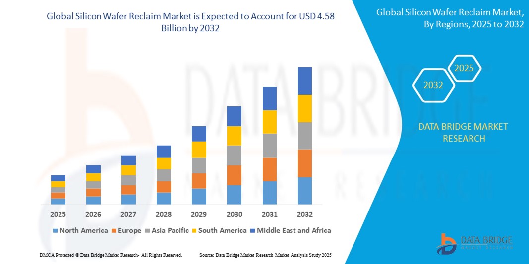
Global Silicon Wafer Reclaim Market Size
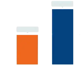
- The Global Silicon Wafer Reclaim Market Size was valued at USD 0.64 Billion in 2024 and is expected to reach USD 4.58 Billion by 2032, at a CAGR of 32.5% during the forecast period
- The growth of the Global Silicon Wafer Reclaim Market is fueled by increasing demand for cost-effective semiconductor manufacturing, sustainability initiatives, and rising adoption of renewable energy technologies like solar power.
Global Silicon Wafer Reclaim Market Analysis
The Global Silicon Wafer Reclaim Market is experiencing steady growth, driven by the increasing demand for cost-effective semiconductor manufacturing and sustainability initiatives within the electronics industry. As the global demand for consumer electronics, automotive semiconductors, and photovoltaic cells rises, manufacturers are focusing on reducing production costs and environmental impact. Reclaimed silicon wafers, which are recycled and reprocessed from used wafers for use in monitoring and testing, offer a compelling solution. This enables fabs to reuse materials without compromising process control, lowering material costs and waste.
Key industries such as consumer electronics, automotive, and solar energy are fueling this growth due to their dependence on advanced semiconductors and their alignment with green manufacturing trends. Additionally, the expansion of 5G, IoT, and AI-based technologies has intensified the need for semiconductors, indirectly supporting the reclaim market. Wafer reclaim also aligns with global ESG goals, contributing to circular economy strategies and appealing to companies focused on responsible resource utilization.
Technological advancements in reclaim processes such as improved wafer polishing, cleaning, and inspection techniques have significantly enhanced the quality of reclaimed wafers, making them suitable for high-precision applications. Furthermore, the increasing use of 300mm wafers in modern fabs has created opportunities for specialized reclaim services.
However, the market also faces challenges. The precision required in reclaiming wafers, the risk of contamination, and the need for stringent quality control remain significant barriers. Additionally, not all used wafers are suitable for reclaiming, and specialized equipment and expertise are necessary to ensure consistent output, which can restrict entry for new players.
Report Scope and Global Silicon Wafer Reclaim Market Segmentation
|
Attributes |
Global Silicon Wafer Reclaim Market Insights |
|
Segments Covered |
|
|
Countries Covered |
North America
Europe
Asia-Pacific
Middle East and Africa
South America
|
|
Key Market Players |
|
|
Market Opportunities |
|
|
Value Added Data Infosets |
In addition to the insights on market scenarios such as market value, growth rate, segmentation, geographical coverage, and major players, the market reports curated by the Data Bridge Market Research also include in-depth expert analysis, pricing analysis, brand share analysis, consumer survey, demography analysis, supply chain analysis, value chain analysis, raw material/consumables overview, vendor selection criteria, PESTLE Analysis, Porter Analysis, and regulatory framework. |
Global Silicon Wafer Reclaim Market Trends
“Sustainability and Technological Advancements Reshaping Wafer Reclaim Practices”
- A major and evolving trend in the Global Silicon Wafer Reclaim Market is the increasing emphasis on sustainable manufacturing practices. Semiconductor manufacturers are adopting wafer reclaiming as part of their ESG goals to reduce waste and carbon footprint while optimizing resource utilization.
- Technological advancements in wafer polishing, surface conditioning, and particle inspection are enabling higher-quality reclaimed wafers that can meet the rigorous standards of semiconductor fabs, thereby increasing acceptance and usability.
- The growing demand for 300mm and larger wafer sizes in semiconductor production is pushing reclaim service providers to upgrade their facilities with more automated and precision-driven equipment.
- Integration of AI-driven quality inspection and data analytics tools is enabling real-time defect detection, improving process efficiency, and reducing reclaim cycle times.
- With the rise of IoT, 5G, and AI-driven devices, the demand for cost-effective testing wafers has surged—driving the use of reclaimed wafers in monitoring and test processes, especially for advanced node fabrication.
Global Silicon Wafer Reclaim Market Dynamics
Driver
“Rising Demand for Cost Efficiency, Circular Economy, and Semiconductor Innovation”
- The rising cost of prime silicon wafers and the increasing focus on sustainable manufacturing are driving semiconductor companies to adopt wafer reclaiming as a cost-effective and environmentally responsible alternative.
- The expansion of the global semiconductor industry, driven by demand for smartphones, EVs, AI, and IoT devices, is increasing the need for reclaimed wafers for equipment monitoring, testing, and process qualification.
- Government regulations and industry-wide sustainability goals are encouraging companies to reduce silicon waste and energy use, boosting the appeal of reclaim and reuse strategies.
- Advancements in reclaim technologies—such as improved wafer stripping, polishing, and inspection—are enabling better quality control and wider application of reclaimed wafers across 150mm, 200mm, and 300mm formats.
- The growth of semiconductor fabs in emerging markets such as Southeast Asia, India, and Eastern Europe is opening new opportunities for regional reclaim service providers and partnerships with foundries and IDMs.
Restraint/Challenge
“High Cost, Technical Complexity, and Limited Adoption in Developing Economies”
- The high capital investment required for reclaiming equipment such as stripping tools, polishing systems, and advanced metrology tools presents a significant entry barrier for small and mid-sized reclaim facilities.
- Technical complexity in achieving defect-free reclaim wafers, especially for advanced nodes, poses challenges in maintaining quality standards for reuse in critical process applications.
- Limited awareness about the economic and environmental benefits of wafer reclaim particularly in developing countries restricts broader market penetration.
- Inconsistent global standards for wafer reclaim processes, and lack of certifications in emerging markets, hinder uniformity in reclaim quality and reduce cross-border demand.
- Handling ultra-thin wafers or wafers with complex materials (e.g., SOI, GaN) introduces reliability risks, demanding highly controlled environments and skilled personnel for effective reclaim.
Global Silicon Wafer Reclaim Market Scope
The market is segmented on the basis of Wafer Diameter, Reclaim Method, Technology Process and
End-User Industry
By Wafer Diameter
The Global Silicon Wafer Reclaim Market, based on wafer diameter, is categorized into less than 200 mm, 200–300 mm, and greater than 300 mm segments. The <200 mm segment caters to older-generation semiconductor applications, including automotive, analog devices, MEMS, and power electronics. These wafers are widely reclaimed due to their cost sensitivity and widespread use in industrial and consumer electronics. Despite lower performance compared to larger wafers, their reclaimability makes them essential in cost-driven sectors. The 200–300 mm segment dominates the market, owing to its broad adoption in mainstream semiconductor manufacturing. Foundries and integrated device manufacturers (IDMs) widely utilize these wafers for producing logic, memory, and power ICs. Reclaiming 200–300 mm wafers offers significant savings and supports sustainability initiatives, making it the most lucrative segment. The >300 mm segment, though still nascent, is poised for long-term growth. These larger wafers are primarily used in advanced, high-density semiconductor fabrication, including for AI, HPC, and data center applications. As the semiconductor industry gradually moves towards 450 mm wafer production, this segment will become more prominent, driven by efficiency and yield advantages. However, reclaim processes for >300 mm wafers are more complex and still under development.
- By Reclaim Method
Based on reclaim method, the Global Silicon Wafer Reclaim Market is segmented into Mechanical and Chemical processes. The Mechanical reclaim method involves physical techniques such as grinding, polishing, and cleaning to remove surface layers and defects from used wafers. This method is cost-effective and widely adopted for wafers with minor damage or limited contamination. It is favored in applications where reclaimed wafers are used for non-critical processes like equipment calibration, monitoring, or as test wafers. The Chemical reclaim method uses chemical etching, stripping, and cleaning processes to remove layers from the wafer surface. This method is more precise and suitable for reclaiming wafers with heavy contamination or intricate circuit patterns. It allows for better surface quality and reuse in more advanced semiconductor processes. Chemical reclaim is gaining traction due to its effectiveness in maintaining wafer integrity and performance, despite being more expensive and complex.
- By Technology Process
The Global Silicon Wafer Reclaim Market, when segmented by technology process, includes Photolithography, Chemical Vapor Deposition (CVD), Etching, Ion Implantation, and Thin-film Deposition. Each of these processes plays a vital role in semiconductor manufacturing and significantly benefits from reclaimed wafers. In photolithography, reclaimed wafers are used to test alignment and pattern accuracy, reducing the need for new, expensive wafers during process trials. CVD processes utilize reclaimed wafers to evaluate film deposition uniformity and thickness without compromising production resources. Similarly, in etching, these wafers are instrumental in developing etch recipes and monitoring etch rates. Ion implantation benefits from reclaimed wafers by using them in beam calibration and dopant profiling, helping improve accuracy while minimizing waste. Lastly, thin-film deposition processes, including sputtering and evaporation, leverage reclaimed wafers to assess film adhesion, consistency, and stress performance. This segmentation highlights the critical role of reclaimed wafers in optimizing production efficiency, reducing costs, and supporting equipment calibration across multiple advanced semiconductor fabrication processes.
- By End-User Industry
The Global Silicon Wafer Reclaim Market, by end-user industry, is segmented into Semiconductor Manufacturers, Integrated Device Manufacturers (IDMs), Consumer Electronics, Automotive Electronics, Solar Energy, and Telecommunications. Semiconductor manufacturers and IDMs represent the largest share due to their continuous demand for cost-effective wafer recycling solutions in process testing, tool calibration, and equipment maintenance. Consumer electronics drive demand through high-volume production of devices such as smartphones, tablets, and laptops, where wafer reclaim helps reduce production costs. The automotive electronics sector is also expanding rapidly, fueled by the growth of electric vehicles (EVs) and advanced driver-assistance systems (ADAS), which rely on precise and affordable semiconductor testing solutions. In the solar energy industry, reclaimed wafers are increasingly used for testing photovoltaic cell production processes and material efficiency. Lastly, the telecommunications segment benefits from reclaimed wafers in the development of high-frequency and 5G-enabled chips, supporting R&D efforts while maintaining budget constraints. This segmentation underscores how a broad range of technology-driven industries are adopting silicon wafer reclaim to enhance sustainability and cost-effectiveness.
Global Silicon Wafer Reclaim Market Regional Analysis
- North America accounts for roughly 25% of the global wafer reclaim market, propelled by its mature semiconductor ecosystem and strong emphasis on sustainability. The U.S. leads the region, with major fabs (like Intel, GlobalFoundries) adopting reclaimed wafers for tool calibration and testing, driven by cost-efficiency, environmental regulations, and initiatives like the U.S. CHIPS Act.
- Europe contributes about 20% of the market, driven primarily by its robust automotive and industrial electronics sectors. Germany and the U.K. stand out for their focus on resource optimization and green manufacturing, using reclaimed wafers to reduce production costs while complying with strict environmental standards.
- Asia Pacific is the dominant force, representing 40–70% of the market share. Leading countries China, Japan, South Korea, Taiwan boast advanced semiconductor and solar cell manufacturing infrastructure. Asia Pacific is the fastest-growing region for reclaim wafers due to its vast fabs, cost-sensitive production, and government-backed initiatives.
- Latin America is an emerging market, contributing around 8% of global volume, with key growth in Brazil and Mexico. These markets are expanding in electronics and solar panel deployment, where reclaimed wafers provide an affordable and sustainable solution.
- Middle East & Africa currently makes up around 7–8% of the global market. Growth here is primarily fueled by increasing solar energy projects and expanding electronics manufacturing. Governments in the UAE, Saudi Arabia, and South Africa are promoting sustainability practices that favor wafer reclaim solutions .
North America Silicon Wafer Reclaim Market Insight
The North America Silicon Wafer Reclaim Market is experiencing steady growth, driven by increasing demand for cost-effective and sustainable wafer reuse in the semiconductor industry. The U.S. leads regional growth due to the presence of major semiconductor manufacturers and government initiatives like the CHIPS Act that promote domestic production and recycling. The 300 mm wafer segment dominates the market due to its widespread use in advanced chip manufacturing. Additionally, strong regulatory support for circular economy practices and growing adoption of eco-friendly manufacturing technologies are further fueling market expansion across North America.
Europe Silicon Wafer Reclaim Market Insight
The Europe silicon wafer reclaim market is experiencing steady growth, driven by the region’s strong focus on sustainability, cost-efficiency, and technological advancement. Countries like Germany, France, and the UK are leading in reclaim adoption due to their robust semiconductor manufacturing and automotive electronics sectors. The growing emphasis on recycling and green manufacturing practices is encouraging semiconductor fabs to adopt wafer reclaiming to reduce material waste and minimize environmental impact. Additionally, increased research and development activities, supported by the European Union’s funding for semiconductor innovation, are boosting the use of reclaimed wafers in testing, calibration, and non-critical production processes. The demand is further reinforced by rising technological integration across industries such as telecommunications, renewable energy, and consumer electronics.
Asia Pacific Silicon Wafer Reclaim Market Insight
The Asia Pacific region leads the silicon wafer reclaim market, fueled by its dominant semiconductor manufacturing industries in countries such as China, Taiwan, South Korea, and Japan. With a strong focus on cost efficiency and high production volumes, wafer reclaiming is widely embraced for equipment calibration, process validation, and reducing raw material consumption. Rapid expansion in device fabrication driven by 5G, AI, electric vehicles, and renewable energy technologies has further elevated the use of reclaimed wafers to support non-critical testing and monitoring. Additionally, government support aimed at promoting semiconductor sovereignty and sustainable manufacturing aligns well with the circular economy benefits of reclaiming. As fabs in the region continue to scale and diversify, both large and mid-size reclaim facilities are investing in advanced reclaim technologies to meet rising demand and enhance process reliability.
Latin America Silicon Wafer Reclaim Market Insight
Latin America’s silicon wafer reclaim market is in the early stages of growth, driven by emerging electronics manufacturing activity and increasing investment in renewable energy sectors. Countries like Brazil and Mexico are beginning to adopt wafer reclaiming practices to reduce production costs and support sustainability initiatives in local semiconductor and solar PV industries. As regional fabs expand capacity, reclaimed wafers are increasingly used for equipment calibration, process development, and photovoltaic cell production. While adoption remains modest due to limited reclaim infrastructure and market awareness, government incentives in clean energy and digitalization are fostering interest. Going forward, coordinated efforts between fab operators, research institutions, and policymakers will be essential to scale reclaim operations and embed circular economy practices in the region’s semiconductor ecosystem.
Middle East and Africa Silicon Wafer Reclaim Market Insight
The silicon wafer reclaim market in the Middle East and Africa is emerging, driven primarily by initial investments in solar PV manufacturing, electronics assembly, and research facilities. Nations like the UAE, South Africa, and Saudi Arabia are gradually exploring wafer reclaim technologies to support sustainability goals and reduce waste in nascent semiconductor-related operations. Reclaimed wafers are increasingly being used for equipment calibration and testing in these facilities, offering cost-efficient alternatives to new wafers. However, challenges such as limited technical expertise, lack of reclaim infrastructure, and varying policy support across the region hinder rapid adoption. As governments advance industrialization and circular economy initiatives, collaboration between fab operators, clean-tech providers, and academic institutions will be critical to scale reclaiming capabilities and establish sustainable practices in the MEA semiconductor supply chain.
Global Silicon Wafer Reclaim Market Share
The Global Silicon Wafer Reclaim industry is primarily led by well-established companies, including:
- Pure Wafer
- RS Technologies
- Nano Silicon
- Advantec
- KST World Corp
- Noel Technologies
- Phoenix Silicon International
- Optim Wafer Services
- Silicon Valley Microelectronics
- Shinryo Corporation
Latest Developments in Global Silicon Wafer Reclaim Market
- In May 2024, NanoSilicon Corp., a leading silicon wafer reclaim service provider, unveiled its next-generation reclaim process capable of achieving ultra-low particle counts on 300 mm wafers. This innovation aims to meet the increasing quality demands of advanced semiconductor manufacturing while enhancing reclaim efficiency and reducing processing time.
- In March 2024, RS Technologies Co., Ltd. announced the expansion of its reclaim facility in Taiwan, driven by increased demand from foundries and integrated device manufacturers (IDMs) in the Asia-Pacific region. The new line focuses on reclaiming 200 mm and 300 mm wafers with advanced chemical cleaning and polishing technologies.
- In January 2024, Pure Wafer, a U.S.-based silicon wafer reclaim company, entered a strategic alliance with a leading solar panel manufacturer to provide reclaimed wafers for non-critical solar applications. The move supports cost reduction and circular economy efforts in the solar industry.
- In November 2023, Shinryo Corporation launched a smart wafer traceability system for its reclaim services, utilizing RFID and blockchain technology to track wafer lifecycle and ensure process transparency for clients in the semiconductor sector.
- In August 2023, GlobalWafers Co., Ltd. invested in AI-driven defect detection systems at its reclaim plants in South Korea and Japan, enhancing inspection accuracy and optimizing wafer recovery rates. This aligns with the company’s push toward digital transformation in wafer services.
SKU-
- Interactive Data Analysis Dashboard
- Company Analysis Dashboard for high growth potential opportunities
- Research Analyst Access for customization & queries
- Competitor Analysis with Interactive dashboard
- Latest News, Updates & Trend analysis
- Harness the Power of Benchmark Analysis for Comprehensive Competitor Tracking
Global Silicon Wafer Reclaim Market, Supply Chain Analysis and Ecosystem Framework
To support market growth and help clients navigate the impact of geopolitical shifts, DBMR has integrated in-depth supply chain analysis into its Global Silicon Wafer Reclaim Market research reports. This addition empowers clients to respond effectively to global changes affecting their industries. The supply chain analysis section includes detailed insights such as Global Silicon Wafer Reclaim Market consumption and production by country, price trend analysis, the impact of tariffs and geopolitical developments, and import and export trends by country and HSN code. It also highlights major suppliers with data on production capacity and company profiles, as well as key importers and exporters. In addition to research, DBMR offers specialized supply chain consulting services backed by over a decade of experience, providing solutions like supplier discovery, supplier risk assessment, price trend analysis, impact evaluation of inflation and trade route changes, and comprehensive market trend analysis.
Data collection and base year analysis are done using data collection modules with large sample sizes. The stage includes obtaining market information or related data through various sources and strategies. It includes examining and planning all the data acquired from the past in advance. It likewise envelops the examination of information inconsistencies seen across different information sources. The market data is analysed and estimated using market statistical and coherent models. Also, market share analysis and key trend analysis are the major success factors in the market report. To know more, please request an analyst call or drop down your inquiry.
The key research methodology used by DBMR research team is data triangulation which involves data mining, analysis of the impact of data variables on the market and primary (industry expert) validation. Data models include Vendor Positioning Grid, Market Time Line Analysis, Market Overview and Guide, Company Positioning Grid, Patent Analysis, Pricing Analysis, Company Market Share Analysis, Standards of Measurement, Global versus Regional and Vendor Share Analysis. To know more about the research methodology, drop in an inquiry to speak to our industry experts.
Data Bridge Market Research is a leader in advanced formative research. We take pride in servicing our existing and new customers with data and analysis that match and suits their goal. The report can be customized to include price trend analysis of target brands understanding the market for additional countries (ask for the list of countries), clinical trial results data, literature review, refurbished market and product base analysis. Market analysis of target competitors can be analyzed from technology-based analysis to market portfolio strategies. We can add as many competitors that you require data about in the format and data style you are looking for. Our team of analysts can also provide you data in crude raw excel files pivot tables (Fact book) or can assist you in creating presentations from the data sets available in the report.


