
Global Thin Wafer Market
Market Size in USD Billion
 USD
11.47 Billion
USD
22.26 Billion
2024
2032
USD
11.47 Billion
USD
22.26 Billion
2024
2032
| 2025 - 2032 | |
| USD 11.47 Billion | |
| USD 22.26 Billion | |
| % | |
|
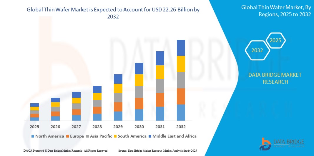
Thin Wafer Market Size
- The global thin wafer market size was valued at USD 11.47 billion in 2024 and is expected to reach USD 22.26 billion by 2032, at a CAGR of 8.64% during the forecast period
- The market growth is largely fuelled by the increasing demand for compact, high-performance semiconductors across consumer electronics, automotive, and industrial applications
- Rising adoption of advanced manufacturing technologies and the push for smaller, lighter, and more energy-efficient wafers are accelerating market expansion
Thin Wafer Market Analysis
- The market is witnessing significant growth due to the rising demand for miniaturized and high-performance semiconductor devices across consumer electronics, automotive, and industrial applications. The shift toward compact and energy-efficient devices is fueling thin wafer adoption
- Advancements in wafer manufacturing technologies, including precision thinning and handling processes, are enhancing product quality, reducing material waste, and supporting large-scale production, thereby positively impacting market growth
- North America dominated the thin wafer market with the largest revenue share of 35.50% in 2024, driven by the presence of advanced semiconductor manufacturing facilities, strong R&D capabilities, and high adoption of consumer electronics
- Asia-Pacific region is expected to witness the highest growth rate in the global thin wafer market, driven by rapid industrialization, expansion of semiconductor fabs in countries such as Taiwan, China, Japan, and South Korea, and increasing adoption of miniaturized, high-performance electronic devices
- The 300 mm segment held the largest market revenue share in 2024, driven by its widespread use in high-performance semiconductor manufacturing and its compatibility with advanced device fabrication processes. 300 mm wafers enable higher throughput, improved yield, and cost efficiency, making them a preferred choice for large-scale production
Report Scope and Thin Wafer Market Segmentation
|
Attributes |
Thin Wafer Key Market Insights |
|
Segments Covered |
|
|
Countries Covered |
North America
Europe
Asia-Pacific
Middle East and Africa
South America
|
|
Key Market Players |
|
|
Market Opportunities |
|
|
Value Added Data Infosets |
In addition to the insights on market scenarios such as market value, growth rate, segmentation, geographical coverage, and major players, the market reports curated by the Data Bridge Market Research also include in-depth expert analysis, geographically represented company-wise production and capacity, network layouts of distributors and partners, detailed and updated price trend analysis and deficit analysis of supply chain and demand. |
Thin Wafer Market Trends
Increasing Adoption of Thin Wafers in Advanced Electronics
- The growing use of thin wafers is transforming the semiconductor and electronics landscape by enabling smaller, lighter, and more energy-efficient devices. Their reduced thickness allows for enhanced thermal performance, improved electrical characteristics, and increased device density, benefiting manufacturers and end-users alike. This trend is further supported by advancements in wafer bonding and packaging technologies, which allow integration into complex semiconductor assemblies
- Rising demand for compact consumer electronics, such as smartphones, wearables, and tablets, is accelerating the adoption of thin wafers. These wafers facilitate higher performance and miniaturization, allowing companies to meet evolving technological and design requirements. In addition, the expansion of IoT devices and 5G-enabled hardware is further driving wafer deployment across multiple applications
- The cost-effectiveness and compatibility of thin wafers with existing fabrication processes make them attractive for high-volume production. Manufacturers can achieve improved yield rates and reduced material usage, supporting sustainable production practices. Coupled with ongoing innovations in lithography and etching, thin wafers help reduce production time and improve overall manufacturing efficiency
- For instance, in 2023, leading semiconductor manufacturers in East Asia reported increased implementation of 200 mm and 300 mm thin wafers in memory and logic devices, enhancing device performance and energy efficiency while reducing production costs. The adoption of these wafers also helped companies meet stringent energy and environmental standards, strengthening their competitive position globally
- While thin wafers offer significant advantages, market growth relies on continued innovation in wafer handling, advanced lithography, and process integration to fully exploit their potential across diverse applications. Investment in automation, defect reduction strategies, and advanced inspection technologies remains critical for sustaining growth
Thin Wafer Market Dynamics
Driver
Rising Demand for Miniaturized and High-Performance Electronic Devices
- The surge in demand for smaller, faster, and more energy-efficient devices is driving the adoption of thin wafers across semiconductor manufacturing. These wafers enable enhanced device performance, increased functionality, and reduced power consumption, meeting end-user expectations. The growing prevalence of AI, high-performance computing, and automotive electronics is also fueling demand for ultra-thin wafers
- Electronics manufacturers are investing in R&D to develop advanced thin wafer technologies compatible with next-generation devices, including AI chips, high-density memory, and IoT sensors. Improved wafer uniformity and reliability further support widespread adoption. Concurrently, wafer suppliers are introducing innovative surface treatments and coatings to enhance electrical and thermal characteristics
- Industry players are focusing on innovations in wafer thinning, precision polishing, and handling techniques, which improve yield rates and reduce material waste, enhancing overall manufacturing efficiency. Advanced robotics and AI-driven wafer handling systems are also being implemented to minimize breakage and contamination, ensuring consistent quality
- For instance, in 2022, several North American and Asian semiconductor fabs implemented ultra-thin wafers for high-performance processors, boosting production capabilities and supporting advanced electronics applications. These fabs also integrated inline monitoring and adaptive process controls to further improve efficiency and reduce production downtime
- While miniaturization drives growth, consistent technological advancements, investment in automation, and process optimization remain essential to sustain market adoption. In addition, collaborations between wafer manufacturers, equipment providers, and device makers are critical for standardizing ultra-thin wafer processes
Restraint/Challenge
High Manufacturing Costs and Technical Complexity
- Thin wafer production involves sophisticated equipment, precise handling, and high-purity materials, making it more expensive than conventional wafer manufacturing. This cost barrier limits adoption among smaller semiconductor producers. Moreover, the need for advanced inspection tools and cleanroom environments further increases operational expenses
- In addition, handling ultra-thin wafers requires specialized machinery and skilled personnel to prevent breakage, warping, or defects. The complexity of integrating thin wafers into standard fabrication lines can hinder production efficiency. Even minor errors in alignment or bonding can result in significant yield losses, affecting profitability
- Supply chain constraints, including limited availability of ultra-pure silicon and advanced polishing tools, can affect timely wafer production and increase lead times, impacting downstream device manufacturing. Geopolitical and trade-related challenges also add uncertainty to wafer material sourcing, potentially delaying large-scale deployments
- For instance, in 2023, semiconductor manufacturers in Southeast Asia reported challenges in scaling production of sub-100 µm wafers due to high equipment costs and technical expertise gaps, slowing expansion in certain markets. Companies also faced difficulties maintaining consistent wafer thickness and surface uniformity, affecting device performance
- Addressing these challenges requires investment in automated handling systems, workforce training, and process innovation to reduce costs, improve yield, and enable broader market penetration. Collaborative research with equipment suppliers, adoption of smart manufacturing techniques, and development of modular production lines are additional strategies to overcome these constraints
Thin Wafer Market Scope
The market is segmented on the basis of wafer size, process, technology, and application.
• By Wafer Size
On the basis of wafer size, the thin wafer market is segmented into 125 mm, 200 mm, and 300 mm. The 300 mm segment held the largest market revenue share in 2024, driven by its widespread use in high-performance semiconductor manufacturing and its compatibility with advanced device fabrication processes. 300 mm wafers enable higher throughput, improved yield, and cost efficiency, making them a preferred choice for large-scale production.
The 200 mm segment is expected to witness the fastest growth rate from 2025 to 2032, fueled by its adoption in MEMS, LED, and sensor manufacturing. 200 mm wafers offer a balance of performance and cost-effectiveness, making them ideal for specialized and medium-volume applications.
• By Process
On the basis of process, the market is segmented into Temporary Bonding & Debonding and Carrier-less/Taiko Process. Temporary Bonding & Debonding held the largest revenue share in 2024, due to its ability to support ultra-thin wafer handling with high precision and minimal breakage. This process is widely adopted for high-density memory and logic device fabrication.
The Carrier-less/Taiko process is expected to witness the fastest growth rate from 2025 to 2032, driven by its advantages in reducing warpage and improving surface uniformity, which are critical for MEMS and LED applications.
• By Technology
On the basis of technology, the market is segmented into Wafer Grinding, Wafer Polishing, and Wafer Dicing. Wafer Grinding accounted for the largest revenue share in 2024, owing to its role in achieving precise wafer thickness and uniformity for high-performance devices. Advanced grinding techniques improve yield and device reliability.
Wafer Polishing is expected to witness the fastest growth rate from 2025 to 2032, fueled by the increasing demand for smooth, defect-free wafer surfaces necessary for MEMS, CIS, and LED devices.
• By Application
On the basis of application, the market is segmented into MEMS, CIS, Memory, RF Devices, LED, Interposer, and Logic. The Memory segment held the largest market share in 2024, driven by high adoption in DRAM, NAND, and emerging high-density memory devices. Thin wafers enable increased integration and device miniaturization.
The MEMS segment is expected to witness the fastest growth rate from 2025 to 2032, propelled by rising demand in automotive, consumer electronics, and industrial sensors that require compact and highly precise components.
Thin Wafer Market Regional Analysis
- North America dominated the thin wafer market with the largest revenue share of 35.50% in 2024, driven by the presence of advanced semiconductor manufacturing facilities, strong R&D capabilities, and high adoption of consumer electronics
- Manufacturers in the region highly value the efficiency, precision, and compatibility offered by thin wafers for high-performance devices, supporting miniaturization and energy efficiency
- This widespread adoption is further supported by robust industrial infrastructure, high investment in semiconductor research, and the increasing demand for compact and high-speed electronic devices, establishing thin wafers as a critical component in the region’s electronics ecosystem
U.S. Thin Wafer Market Insight
The U.S. thin wafer market captured the largest revenue share in 2024 within North America, fueled by rapid advancements in semiconductor fabrication and the growing production of high-performance processors, memory, and logic devices. Manufacturers are increasingly prioritizing the use of ultra-thin wafers to achieve higher device density, better thermal performance, and improved electrical characteristics. The rising integration of thin wafers in advanced electronics, including AI chips, IoT devices, and wearable technology, is significantly contributing to the market’s expansion.
Europe Thin Wafer Market Insight
The Europe thin wafer market is expected to witness the fastest growth rate from 2025 to 2032, primarily driven by the increasing adoption of miniaturized electronics and high-precision semiconductor components. The region’s focus on advanced manufacturing techniques, such as wafer thinning, grinding, and polishing, is fostering the demand for thin wafers. European consumers and industries are also drawn to the enhanced energy efficiency and reliability that thin wafers offer. The market is witnessing growth across applications including MEMS, LED, RF devices, and interposer technologies.
U.K. Thin Wafer Market Insight
The U.K. thin wafer market is expected to witness the fastest growth rate from 2025 to 2032, driven by the expanding electronics and semiconductor sectors. The rising demand for high-performance computing, memory solutions, and consumer electronics is encouraging manufacturers to adopt thin wafer technologies. In addition, government support for semiconductor R&D and the presence of advanced fabrication facilities is expected to continue stimulating market growth.
Germany Thin Wafer Market Insight
The Germany thin wafer market is expected to witness the fastest growth rate from 2025 to 2032, fueled by the country’s emphasis on innovation, precision engineering, and energy-efficient semiconductor solutions. Germany’s well-developed industrial infrastructure, combined with the adoption of cutting-edge wafer processing technologies, promotes the integration of thin wafers across electronics applications. The market is increasingly focusing on MEMS, LED, RF devices, and logic applications, reflecting strong alignment with local technological trends.
Asia-Pacific Thin Wafer Market Insight
The Asia-Pacific thin wafer market is expected to witness the fastest growth rate from 2025 to 2032, driven by rapid industrialization, urbanization, and the expanding electronics and semiconductor manufacturing base in countries such as China, Japan, South Korea, and Taiwan. The region’s growing inclination towards high-performance devices, smart electronics, and wearable technology is driving adoption. Furthermore, Asia-Pacific serves as a manufacturing hub for thin wafers and semiconductor components, increasing affordability, accessibility, and adoption across global supply chains.
Japan Thin Wafer Market Insight
The Japan thin wafer market is expected to witness the fastest growth rate from 2025 to 2032 due to the country’s high-tech culture, strong semiconductor industry, and demand for compact, energy-efficient devices. Japanese manufacturers emphasize wafer uniformity, advanced polishing, and carrier-less processes, enabling the production of high-performance processors, memory chips, and MEMS devices. The integration of thin wafers with IoT devices, AI processors, and automotive electronics is further fueling market growth.
China Thin Wafer Market Insight
The China thin wafer market accounted for the largest market revenue share in Asia Pacific in 2024, attributed to the country’s rapidly growing semiconductor industry, strong R&D capabilities, and expanding electronics manufacturing base. China is one of the largest producers and consumers of semiconductors, and thin wafers are increasingly adopted in memory, logic, and CIS applications. The push towards advanced electronics manufacturing, smart devices, and domestic semiconductor self-reliance, alongside competitive wafer pricing and local production capacity, are key factors propelling the market in China.
Thin Wafer Market Share
The Thin Wafer industry is primarily led by well-established companies, including:
- Shin-Etsu Chemical Co., Ltd. (Japan)
- SUMCO Corporation (Japan)
- GlobalWafers Co., Ltd. (Taiwan)
- Siltronic (Germany)
- SK Siltron (South Korea)
- SUSS MicroTec (Germany)
- Soitec (France)
- DISCO Corporation (Japan)
- 3M (U.S.)
- Applied Materials (U.S.)
- Mechatronic Systerntechnik (Austria)
- Synova (Switzerland)
- Brewer Science (U.S.)
- EV Group (Austria)
- Wafer Works Corporation (Taiwan)
- Atecom Technology Co., Ltd. (Taiwan)
- Siltronix Silicon Technologies (France)
- LDK Solar (China)
- UniversityWafer, Inc. (U.S.)
- Wafer World Inc. (U.S.)
- Silicon Valley Microelectronics (U.S.)
- Shanghai Simgui Technology Co., Ltd. (China)
- PV Crystalox Solar PLC (U.K.)
Latest Developments in Global Thin Wafer Market
- In February 2022, Shin-Etsu Chemical Co., Ltd. (Japan) announced a major facility investment of over YEN 80 billion in its silicones business, aiming to expand production capacity and strengthen its core operations, supporting long-term growth and enhancing its position in the global semiconductor materials market
- In October 2022, Siltronic (Germany) commenced construction of a new manufacturing facility at JTC’s Tampines Wafer Fab Park in Singapore, in collaboration with the Singapore Economic Development Board (EDB), with an investment of approximately EUR 2 billion, expected to boost wafer production capabilities and meet rising semiconductor demand in Asia-Pacific
- In February 2021, Siltronic and GlobalWafers Co., Ltd. (Taiwan) finalized an agreement providing job security for Siltronic’s German sites until the end of 2024, while combining complementary product portfolios to strengthen market competitiveness and leverage long-term growth opportunities in the global wafer industry
SKU-
- Interactive Data Analysis Dashboard
- Company Analysis Dashboard for high growth potential opportunities
- Research Analyst Access for customization & queries
- Competitor Analysis with Interactive dashboard
- Latest News, Updates & Trend analysis
- Harness the Power of Benchmark Analysis for Comprehensive Competitor Tracking
Global Thin Wafer Market, Supply Chain Analysis and Ecosystem Framework
To support market growth and help clients navigate the impact of geopolitical shifts, DBMR has integrated in-depth supply chain analysis into its Global Thin Wafer Market research reports. This addition empowers clients to respond effectively to global changes affecting their industries. The supply chain analysis section includes detailed insights such as Global Thin Wafer Market consumption and production by country, price trend analysis, the impact of tariffs and geopolitical developments, and import and export trends by country and HSN code. It also highlights major suppliers with data on production capacity and company profiles, as well as key importers and exporters. In addition to research, DBMR offers specialized supply chain consulting services backed by over a decade of experience, providing solutions like supplier discovery, supplier risk assessment, price trend analysis, impact evaluation of inflation and trade route changes, and comprehensive market trend analysis.
Data collection and base year analysis are done using data collection modules with large sample sizes. The stage includes obtaining market information or related data through various sources and strategies. It includes examining and planning all the data acquired from the past in advance. It likewise envelops the examination of information inconsistencies seen across different information sources. The market data is analysed and estimated using market statistical and coherent models. Also, market share analysis and key trend analysis are the major success factors in the market report. To know more, please request an analyst call or drop down your inquiry.
The key research methodology used by DBMR research team is data triangulation which involves data mining, analysis of the impact of data variables on the market and primary (industry expert) validation. Data models include Vendor Positioning Grid, Market Time Line Analysis, Market Overview and Guide, Company Positioning Grid, Patent Analysis, Pricing Analysis, Company Market Share Analysis, Standards of Measurement, Global versus Regional and Vendor Share Analysis. To know more about the research methodology, drop in an inquiry to speak to our industry experts.
Data Bridge Market Research is a leader in advanced formative research. We take pride in servicing our existing and new customers with data and analysis that match and suits their goal. The report can be customized to include price trend analysis of target brands understanding the market for additional countries (ask for the list of countries), clinical trial results data, literature review, refurbished market and product base analysis. Market analysis of target competitors can be analyzed from technology-based analysis to market portfolio strategies. We can add as many competitors that you require data about in the format and data style you are looking for. Our team of analysts can also provide you data in crude raw excel files pivot tables (Fact book) or can assist you in creating presentations from the data sets available in the report.


