
Global Semiconductor Wafer Polishing And Grinding Equipment Market
Market Size in USD Billion
 USD
2.81 Billion
USD
3.71 Billion
2024
2032
USD
2.81 Billion
USD
3.71 Billion
2024
2032
| 2025 - 2032 | |
| USD 2.81 Billion | |
| USD 3.71 Billion | |
| % | |
|
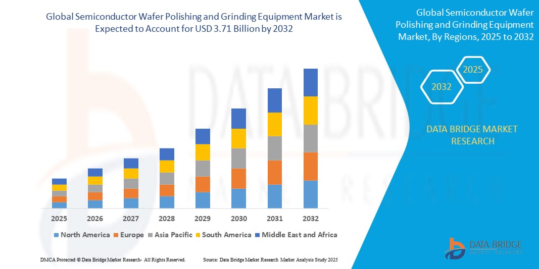
Semiconductor Wafer Polishing and Grinding Equipment Market Size
- The global semiconductor wafer polishing and grinding equipment market size was valued at USD 2.81 billion in 2024 and is expected to reach USD 3.71 billion by 2032, at a CAGR of 3.55% during the forecast period
- The market growth is largely fueled by the increasing demand for high-performance and miniaturized semiconductor devices, which require precise wafer surface processing for advanced node fabrication and 3D integration
- Furthermore, the shift toward heterogeneous integration, advanced packaging, and thinner wafers is accelerating the adoption of wafer polishing and grinding equipment, as these systems ensure defect-free surfaces, optimal flatness, and enhanced yield in complex chip architectures
Semiconductor Wafer Polishing and Grinding Equipment Market Analysis
- Wafer polishing and grinding equipment is used to smooth, thin, and prepare semiconductor wafers for subsequent processing steps, such as lithography, etching, and packaging. These tools are essential for achieving the necessary wafer planarity, surface quality, and dimensional accuracy in advanced chip manufacturing
- The growing need for ultra-thin wafers in applications such as 5G, AI, and advanced computing, along with increased investments in new fabs and the expansion of 3D NAND and logic chip production, are key drivers fueling the demand for wafer polishing and grinding systems across global semiconductor ecosystems
- Asia-Pacific dominated the semiconductor wafer polishing and grinding equipment market with a share of 69.2% in 2024, due to the concentration of major foundries and memory manufacturers in the region
- North America is expected to be the fastest growing region in the semiconductor wafer polishing and grinding equipment market during the forecast period due to government-backed initiatives and large-scale private investments to boost domestic chip manufacturing
- Deposition segment dominated the market with a market share of 35.1% in 2024, due to its critical role in forming thin films and layers during integrated circuit fabrication. Deposition equipment is indispensable for achieving precise material layering required in advanced node technologies, which has led to its broad adoption among chipmakers focusing on performance enhancement and miniaturization. The high usage of deposition tools in both logic and memory applications further reinforces its dominance, particularly as demand for 3D structures and high-density packaging continues to rise
Report Scope and Semiconductor Wafer Polishing and Grinding Equipment Market Segmentation
|
Attributes |
Semiconductor Wafer Polishing and Grinding Equipment Key Market Insights |
|
Segments Covered |
|
|
Countries Covered |
North America
Europe
Asia-Pacific
Middle East and Africa
South America
|
|
Key Market Players |
|
|
Market Opportunities |
|
|
Value Added Data Infosets |
In addition to the insights on market scenarios such as market value, growth rate, segmentation, geographical coverage, and major players, the market reports curated by the Data Bridge Market Research also include in-depth expert analysis, geographically represented company-wise production and capacity, network layouts of distributors and partners, detailed and updated price trend analysis and deficit analysis of supply chain and demand. |
Semiconductor Wafer Polishing and Grinding Equipment Market Trends
“Increasing Demand for Advanced Consumer Electronics”
- The market is experiencing robust growth as the global appetite for advanced consumer electronics—such as smartphones, tablets, wearables, and laptops—continues to surge, driving the need for highly precise and reliable semiconductor components
- For instance, companies such as Applied Materials are expanding their equipment portfolios to cater to the rapidly evolving requirements of consumer electronics manufacturers, offering next-generation polishing and grinding systems that support ultra-thin wafers and advanced chip architectures
- The proliferation of technologies such as 5G, artificial intelligence (AI), and the Internet of Things (IoT) is accelerating demand for more sophisticated semiconductor devices, which in turn requires highly accurate wafer finishing processes to ensure optimal device performance
- The expansion of electric vehicles (EVs), autonomous driving systems, and high-performance computing is further boosting demand for semiconductor wafers with exceptional surface quality and minimal defects, placing greater emphasis on advanced polishing and grinding equipment
- Digital transformation and the rise of data centers are prompting semiconductor manufacturers to invest in state-of-the-art wafer processing equipment to achieve higher yields, improved efficiency, and faster production cycles
- Sustainability initiatives and stricter regulatory standards are encouraging equipment makers to develop solutions that minimize material waste, reduce energy consumption, and support greener manufacturing practices across the semiconductor value chain
Semiconductor Wafer Polishing and Grinding Equipment Market Dynamics
Driver
“Escalating Demand for Semiconductors”
- The global surge in semiconductor consumption, fueled by the proliferation of smart devices, automotive electronics, industrial automation, and renewable energy applications, is a primary driver for the wafer polishing and grinding equipment market
- For instance, Lam Research has reported a substantial increase in orders for its wafer processing equipment from leading foundries and integrated device manufacturers (IDMs), reflecting the industry’s urgent need to scale up production and meet growing chip demand
- The ongoing miniaturization of semiconductor devices, alongside the transition to advanced process nodes and larger wafer sizes (such as 300 mm and 450 mm), is intensifying the need for ultra-precise polishing and grinding solutions that can deliver consistent results at higher volumes
- Rapid advancements in semiconductor manufacturing technologies, including the adoption of automation, real-time process analytics, and AI-based quality control, are driving investment in next-generation wafer finishing equipment that enhances throughput and yield
- The expansion of semiconductor applications into new domains—such as healthcare, smart infrastructure, and next-gen mobility—continues to broaden the customer base for wafer polishing and grinding equipment, underpinning long-term market growth
Restraint/Challenge
“High Initial Investment”
- The high upfront costs associated with acquiring, installing, and maintaining advanced wafer polishing and grinding equipment represent a significant barrier for many semiconductor manufacturers, especially smaller players and new entrants
- For instance, smaller foundries and OSAT (Outsourced Semiconductor Assembly and Test) companies often face challenges in justifying the capital expenditure required for state-of-the-art equipment from leading suppliers such as Ebara or Disco Corporation, which can impact their competitiveness and scalability
- The complexity of integrating new equipment into existing production lines, along with the need for specialized technical expertise and training, can further elevate the total cost of ownership and slow down adoption rates among cost-sensitive manufacturers
- Rapid technological evolution in wafer processing tools means that equipment can become obsolete relatively quickly, increasing the risk associated with large capital investments and pressuring companies to continually upgrade their assets to remain competitive
- Market volatility, supply chain disruptions, and fluctuating demand cycles in the semiconductor industry can make it difficult for manufacturers to forecast returns on investment, leading to cautious spending on new equipment and delayed expansion plans
Semiconductor Wafer Polishing and Grinding Equipment Market Scope
The market is segmented on the basis of equipment and end-users.
- By Equipment
On the basis of equipment, the semiconductor wafer polishing and grinding equipment market is segmented into deposition, lithography, ion implant, etching and cleaning, and others. The deposition segment held the largest market revenue share of 35.1% in 2024, owing to its critical role in forming thin films and layers during integrated circuit fabrication. Deposition equipment is indispensable for achieving precise material layering required in advanced node technologies, which has led to its broad adoption among chipmakers focusing on performance enhancement and miniaturization. The high usage of deposition tools in both logic and memory applications further reinforces its dominance, particularly as demand for 3D structures and high-density packaging continues to rise.
The etching and cleaning segment is projected to witness the fastest growth rate from 2025 to 2032, driven by increasing process complexity and stringent requirements for surface purity and pattern fidelity in sub-7nm nodes. The growth is also fueled by the rising prevalence of 3D NAND and FinFET architectures, where precise etching and post-process cleaning are critical for yield optimization. As device geometries shrink, advanced cleaning technologies capable of minimizing particle contamination and defects are in high demand, pushing this segment's technological and commercial expansion.
- By End-Users
On the basis of end-users, the market is segmented into foundries, memory manufacturers, IDMs, and others. The foundries segment accounted for the largest revenue share in 2024, attributed to the increasing outsourcing of semiconductor production by fabless companies and the rise of leading foundry players investing in next-generation process nodes. Foundries are at the forefront of technological innovation, often pioneering adoption of the latest wafer processing equipment to stay competitive in high-performance computing, AI, and mobile markets. Their continual capital expenditure on polishing and grinding tools to support advanced packaging and wafer thinning processes significantly drives demand.
The memory manufacturers segment is expected to register the fastest growth from 2025 to 2032, propelled by surging global demand for DRAM and NAND flash memory used in data centers, smartphones, and emerging technologies such as automotive AI and IoT. As memory devices become more complex and layered, manufacturers are increasingly investing in ultra-precise grinding and polishing tools to ensure planarization, reduce defect rates, and enable stacking. This rising demand for high-capacity and high-performance memory is accelerating equipment adoption across major memory fabrication facilities.
Semiconductor Wafer Polishing and Grinding Equipment Market Regional Analysis
- Asia-Pacific dominated the semiconductor wafer polishing and grinding equipment market with the largest revenue share of 69.2% in 2024, driven by the concentration of major foundries and memory manufacturers in the region
- The region benefits from robust government support for semiconductor self-sufficiency, rapid technological advancements, and rising demand for consumer electronics and electric vehicles
- Growing investments in new fab constructions, along with a well-established supply chain for semiconductor components and materials, are significantly boosting the adoption of wafer polishing and grinding equipment
China Semiconductor Wafer Polishing and Grinding Equipment Market Insight
China accounted for the largest market share in Asia-Pacific in 2024, supported by ambitious national initiatives such as “Made in China 2025” and substantial investments in domestic semiconductor manufacturing. The rapid expansion of local foundries and memory fabs, combined with the country’s strong focus on developing advanced process nodes, is driving the demand for wafer polishing and grinding equipment. China's leadership in 3D NAND and DRAM manufacturing, along with increasing adoption of AI, IoT, and smart mobility solutions, is accelerating the need for planarization and surface finishing tools across both logic and memory chip production lines.
Japan Semiconductor Wafer Polishing and Grinding Equipment Market Insight
Japan is experiencing consistent growth in the market, fueled by its legacy of innovation in semiconductor materials and equipment. The country plays a vital role in supplying precision tools to global chipmakers and is heavily investing in cutting-edge technologies such as 2nm and below. With a strong domestic demand for automotive and industrial semiconductors, Japan continues to modernize its fabrication processes. Strategic collaborations with international semiconductor leaders and the integration of polishing and grinding equipment into new fab projects are expected to further bolster Japan’s market share over the coming years.
North America Semiconductor Wafer Polishing and Grinding Equipment Market Insight
North America is projected to grow at the fastest CAGR from 2025 to 2032, driven by government-backed initiatives and large-scale private investments to boost domestic chip manufacturing. Programs such as the CHIPS and Science Act are encouraging the development of new semiconductor facilities and advanced packaging centers across the region. The growing need for high-performance computing, AI workloads, and defense-related semiconductor applications is prompting the widespread adoption of precision wafer processing tools. North America’s innovation ecosystem, coupled with the presence of leading semiconductor equipment manufacturers, is expected to keep the region at the forefront of technological progress in wafer polishing and grinding.
U.S. Semiconductor Wafer Polishing and Grinding Equipment Market Insight
The U.S. captured the highest revenue share within North America, accounting for 83% in 2024, as it aggressively scales its semiconductor production capacity. Major chipmakers are establishing new fabs and expanding existing ones to meet demand across critical industries, including cloud computing, autonomous vehicles, and telecommunications. The U.S. market is also witnessing increasing adoption of advanced wafer thinning and surface finishing techniques to support next-generation chip designs. With robust government funding, rising R&D expenditure, and the integration of AI in chip development, the U.S. is rapidly emerging as a high-growth zone for semiconductor equipment.
Europe Semiconductor Wafer Polishing and Grinding Equipment Market Insight
Europe is expected to witness steady and robust growth throughout the forecast period, supported by coordinated efforts to strengthen its regional semiconductor ecosystem and reduce external dependency. The region’s growing demand for chips in electric vehicles, renewable energy systems, and industrial automation is accelerating investments in wafer fabrication and processing capabilities. Countries such as Germany, France, and the Netherlands are spearheading these efforts by establishing new fabs, enhancing R&D hubs, and forming public-private partnerships. The increasing adoption of EUV lithography and advanced packaging solutions is also amplifying the need for high-precision polishing and grinding equipment to ensure yield and reliability.
Germany Semiconductor Wafer Polishing and Grinding Equipment Market Insight
Germany is leading the European market owing to its strong industrial base, focus on automotive electronics, and commitment to digital innovation. The country’s emphasis on high-efficiency, precision manufacturing is driving demand for advanced wafer processing tools in both existing and upcoming fabs. Government incentives to support local semiconductor initiatives and collaboration with global technology firms are further bolstering growth. As Germany continues to advance its role in the global chip supply chain, demand for polishing and grinding equipment is expected to rise, particularly for use in cutting-edge applications such as power electronics and autonomous driving systems.
Semiconductor Wafer Polishing and Grinding Equipment Market Share
The semiconductor wafer polishing and grinding equipment industry is primarily led by well-established companies, including:
- Applied Materials, Inc. (U.S.)
- EBARA CORPORATION (Japan)
- Lapmaster Wolters (U.S.)
- Entrepix, Inc. (U.S.)
- Revasum (U.S.)
- TOKYO SEIMITSU CO., LTD (Japan)
- Logomatic GmbH (Germany)
- Komatsu NTC (Japan)
- Okamoto Corporation (Japan)
- Amtech Systems, Inc. (U.S.)
- BBS KINMEI CO., LTD. (Japan)
- DYMEK Company Ltd. (Hong Kong)
- Logitech (Switzerland)
- SAMSUNG (South Korea)
- Broadcom (U.S.)
- Qualcomm Technologies, Inc. (U.S.)
- Advanced Micro Devices, Inc. (AMD) (U.S.)
- Apple Inc. (U.S.)
- Marvell (U.S.)
- Xilinx (U.S.)
- NVIDIA Corporation (U.S.)
Latest Developments in Global Semiconductor Wafer Polishing and Grinding Equipment Market
- In December 2024, Tokyo Electron Limited (TEL) launched the Ulucus LX, a cutting-edge system utilizing Extreme Laser Lift Off (ELLO) technology for 300mm wafer-bonded devices. This innovation responds to the rising demand for enhanced semiconductor performance and energy efficiency through 3D integration using permanent wafer bonding. The Ulucus LX consolidates laser beam irradiation, wafer separation, and cleaning into a single platform, leveraging TEL’s proprietary expertise in laser control, wafer separation, and cleaning processes. By replacing multiple conventional steps such as back grinding, polishing, and chemical etching, the system significantly boosts productivity while also reducing environmental impact, marking a pivotal advancement in next-generation semiconductor manufacturing
- In June 2022, Applied Materials announced the acquisition of Picosun Oy, a Finnish semiconductor equipment company. This strategic move aims to enhance Applied Materials' ICAPS (IoT, Communications, Automotive, Power, and Sensors) product offerings and deepen customer engagements by integrating Picosun's advanced atomic layer deposition (ALD) technology into its portfolio
- In February 2022, Revasum secured a growth capital facility from SQN Venture Partners, LLC, valued at up to USD 8 million. This debt financing is intended to accelerate the development of new products and provide working capital to support the company's rapid growth, allowing Revasum to expand its capabilities and market reach
SKU-
- Interactive Data Analysis Dashboard
- Company Analysis Dashboard for high growth potential opportunities
- Research Analyst Access for customization & queries
- Competitor Analysis with Interactive dashboard
- Latest News, Updates & Trend analysis
- Harness the Power of Benchmark Analysis for Comprehensive Competitor Tracking
Global Semiconductor Wafer Polishing And Grinding Equipment Market, Supply Chain Analysis and Ecosystem Framework
To support market growth and help clients navigate the impact of geopolitical shifts, DBMR has integrated in-depth supply chain analysis into its Global Semiconductor Wafer Polishing And Grinding Equipment Market research reports. This addition empowers clients to respond effectively to global changes affecting their industries. The supply chain analysis section includes detailed insights such as Global Semiconductor Wafer Polishing And Grinding Equipment Market consumption and production by country, price trend analysis, the impact of tariffs and geopolitical developments, and import and export trends by country and HSN code. It also highlights major suppliers with data on production capacity and company profiles, as well as key importers and exporters. In addition to research, DBMR offers specialized supply chain consulting services backed by over a decade of experience, providing solutions like supplier discovery, supplier risk assessment, price trend analysis, impact evaluation of inflation and trade route changes, and comprehensive market trend analysis.
Data collection and base year analysis are done using data collection modules with large sample sizes. The stage includes obtaining market information or related data through various sources and strategies. It includes examining and planning all the data acquired from the past in advance. It likewise envelops the examination of information inconsistencies seen across different information sources. The market data is analysed and estimated using market statistical and coherent models. Also, market share analysis and key trend analysis are the major success factors in the market report. To know more, please request an analyst call or drop down your inquiry.
The key research methodology used by DBMR research team is data triangulation which involves data mining, analysis of the impact of data variables on the market and primary (industry expert) validation. Data models include Vendor Positioning Grid, Market Time Line Analysis, Market Overview and Guide, Company Positioning Grid, Patent Analysis, Pricing Analysis, Company Market Share Analysis, Standards of Measurement, Global versus Regional and Vendor Share Analysis. To know more about the research methodology, drop in an inquiry to speak to our industry experts.
Data Bridge Market Research is a leader in advanced formative research. We take pride in servicing our existing and new customers with data and analysis that match and suits their goal. The report can be customized to include price trend analysis of target brands understanding the market for additional countries (ask for the list of countries), clinical trial results data, literature review, refurbished market and product base analysis. Market analysis of target competitors can be analyzed from technology-based analysis to market portfolio strategies. We can add as many competitors that you require data about in the format and data style you are looking for. Our team of analysts can also provide you data in crude raw excel files pivot tables (Fact book) or can assist you in creating presentations from the data sets available in the report.


