
Global Euv Lithography Market
Market Size in USD Billion
 USD
11.26 Billion
USD
48.76 Billion
2024
2032
USD
11.26 Billion
USD
48.76 Billion
2024
2032
| 2025 - 2032 | |
| USD 11.26 Billion | |
| USD 48.76 Billion | |
| % | |
|
EUV Lithography Market Analysis
The Extreme Ultraviolet (EUV) lithography market has emerged as a critical driver in the advancement of the semiconductor industry. EUV lithography enables the production of smaller, more efficient, and powerful microchips by using a 13.5 nm wavelength light source, allowing finer circuit patterns on wafers. This technology has become indispensable for manufacturing advanced processors and memory chips, which are vital for applications in AI, 5G, IoT, and automotive sectors.
Recent advancements in EUV lithography have focused on enhancing the efficiency and precision of high-NA (numerical aperture) systems, enabling even smaller node sizes. Collaborations between key players, such as ASML, Intel, and Imec, have accelerated innovation in this field. High-volume production facilities, such as Intel's USD 18.5 billion facility in Ireland, showcase the growing adoption of EUV technology. Meanwhile, companies such as Samsung and TSMC have leveraged EUV lithography to maintain their leadership in advanced semiconductor manufacturing.
With increasing demand for smaller, high-performance chips, the EUV lithography market is poised for significant growth, playing a pivotal role in shaping the future of the global semiconductor industry.
EUV Lithography Market Size
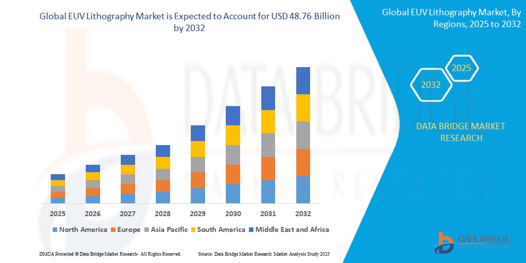
The global EUV lithography market size was valued at USD 11.26 billion in 2024 and is projected to reach USD 48.76 billion by 2032, with a CAGR of 20.10% during the forecast period of 2025 to 2032. In addition to the insights on market scenarios such as market value, growth rate, segmentation, geographical coverage, and major players, the market reports curated by the Data Bridge Market Research also include in-depth expert analysis, geographically represented company-wise production and capacity, network layouts of distributors and partners, detailed and updated price trend analysis and deficit analysis of supply chain and demand.
EUV Lithography Market Trends
“Increasing Demand for Smaller, High-Performance Semiconductors”
The EUV lithography market is witnessing rapid growth, driven by the increasing demand for smaller, high-performance semiconductors in applications such as AI, 5G, and advanced computing. A notable trend shaping this market is the adoption of high-NA EUV lithography systems, which enable the production of chips with even smaller nodes, enhancing device efficiency and functionality. For instance, in June 2024, ASML and Imec established a joint high-NA EUV Lithography Lab, providing a cutting-edge platform for developing next-generation semiconductor technologies. This advancement is critical as manufacturers such as TSMC and Samsung push the boundaries of chip miniaturization to maintain their leadership. High-NA systems also streamline production by reducing complexity, helping foundries meet the growing demand for advanced microchips. As the industry focuses on innovation and collaboration, the EUV lithography market is poised to become a cornerstone for the future of semiconductor manufacturing.
Report Scope and EUV Lithography Market Segmentation
|
Attributes |
EUV Lithography Key Market Insights |
|
Segments Covered |
|
|
Countries Covered |
U.S., Canada and Mexico in North America, Germany, France, U.K., Netherlands, Switzerland, Belgium, Russia, Italy, Spain, Turkey, Rest of Europe in Europe, China, Japan, India, South Korea, Singapore, Malaysia, Australia, Thailand, Indonesia, Philippines, Rest of Asia-Pacific (APAC) in the Asia-Pacific (APAC), Saudi Arabia, U.A.E., South Africa, Egypt, Israel, Rest of Middle East and Africa (MEA) as a part of Middle East and Africa (MEA), Brazil, Argentina and Rest of South America as part of South America |
|
Key Market Players |
Cannon Inc. (Japan), ASML (Netherlands), Nuflare Technology Inc. (Japan), SAMSUNG (South Korea), Intel Corporation (U.S.), Nikon Corporation (Japan), SUSS Microtec SE (Germany), Taiwan Semiconductor Manufacturing Company Limited (Taiwan), Ultratech Inc. (U.S.), Vistec Electron Beam GmbH (Germany), Zeiss International (Germany), Toppan Printing Co. Ltd. (Japan), NTT Advanced Technology Corporation (Japan), Toshiba India Pvt. Ltd. (India), and Global Foundries (U.S.) |
|
Market Opportunities |
|
|
Value Added Data Infosets |
In addition to the insights on market scenarios such as market value, growth rate, segmentation, geographical coverage, and major players, the market reports curated by the Data Bridge Market Research also include in-depth expert analysis, geographically represented company-wise production and capacity, network layouts of distributors and partners, detailed and updated price trend analysis and deficit analysis of supply chain and demand. |
EUV Lithography Market Definition
Extreme Ultraviolet (EUV) lithography is an advanced microfabrication technology used in semiconductor manufacturing to create intricate circuit patterns on silicon wafers. It utilizes a light source with an extremely short wavelength of 13.5 nanometers, enabling the production of smaller and more densely packed transistors compared to traditional lithography methods.
EUV Lithography Market Dynamics
Drivers
- Increased Demand for Advanced semiconductors
The automotive sector is a key driver for the global EUV lithography market, with the increasing demand for advanced semiconductors used in vehicles. Automotive manufacturers are pushing for more sophisticated technologies, and EUV lithography’s ability to produce smaller, more intricate chip designs is essential to meeting these requirements. It enables the creation of high-performance, efficient semiconductor components that are critical for enhancing safety, performance, and functionality in modern vehicles. As the automotive industry evolves towards smarter, connected, and more energy-efficient vehicles, the role of EUV lithography becomes increasingly significant. For instance, Canon’s introduction of the FPA-1200NZ2C system in March 2022 aimed at 5-nanometer chip production reflects the critical role of EUV in enabling cutting-edge semiconductor solutions for automotive applications.
- Rapid Growth of the Consumer Electronics
The rapid growth of the consumer electronics sector, driven by increasing demand for smartphones, wearables, and gaming devices, is a significant driver of the EUV lithography market. Advanced chips used in flagship devices, such as Apple's A17 Bionic (manufactured using TSMC’s 3nm EUV process) and Samsung’s Exynos processors, rely on EUV lithography to achieve superior performance and energy efficiency. As consumer preferences shift toward 5G-enabled and premium devices, semiconductor manufacturers are investing heavily in EUV technology to produce smaller, more efficient chips, linking the rise of consumer electronics directly to the expansion of the EUV lithography market.
Opportunities
- Rising Government Investments
Government investments are significantly contributing to the growth of the EUV lithography market. Many governments worldwide are increasing funding for semiconductor manufacturing and research to bolster their technological advancements and secure a competitive edge in the global market. These investments focus on enabling manufacturers to adopt EUV lithography, which allows the production of high-performance chips with smaller dimensions. As a result, there is a push to accelerate the adoption of EUV technology across various sectors, fostering innovation in industries such as electronics, automotive, and healthcare. For instance, ASML’s initiative in June 2022, collaborating with Mad Science to launch the ASL Junior Academy, highlights efforts to nurture future generations of innovators and engineers, further supporting the advancement of semiconductor technologies.
- Increasing Advanced Semiconductor Manufacturing
As semiconductor technology continues to advance, the need for EUV lithography increases. With the demand for chips with smaller nodes such as 5nm and below EUV lithography is essential in meeting these requirements. It enables the production of microchips with finer features, enhancing performance and energy efficiency in electronic devices. In January 2024, ZEISS Group’s launch of its High-NA EUV lithography system marked a significant advancement in semiconductor manufacturing, supporting the production of chips with unprecedented precision. This technology is pushing the limits of what is possible in chip design, enabling the creation of next-generation semiconductor devices. By enhancing the capabilities of EUV systems, ZEISS contributes to the continued progress in semiconductor technology, fueling growth and innovation in the industry.
Restraints/Challenges
- High Costs of Implementation
The high cost associated with EUV lithography systems is a significant challenge for widespread adoption. The cost of a single EUV machine can exceed USD 100 million, making it prohibitively expensive for smaller semiconductor manufacturers and foundries. This high cost is primarily due to the advanced technology and complex components required to build these machines. Additionally, the limited number of suppliers in the market creates a monopolistic situation that drives prices even higher. Smaller companies often find it difficult to invest in such costly equipment, which consolidates access to EUV technology among larger firms and limits competition. This financial barrier hampers the growth of smaller players, potentially slowing the pace of innovation in the semiconductor industry.
- Limited Supply of EUV Sources
The availability of EUV light sources is another significant constraint for the growth of the EUV lithography market. These light sources are essential for generating the extreme ultraviolet radiation needed for precise chip patterning. However, only a few manufacturers, such as ASML, are currently able to produce these highly specialized light sources, leading to supply limitations. The scarcity of EUV sources restricts the widespread adoption of EUV lithography across the semiconductor industry, slowing advancements in chip production. The high cost and complexity involved in developing and maintaining these light sources further exacerbates supply challenges, limiting the number of companies able to invest in EUV technology. This constraint impedes overall market growth and delays the development of next-generation semiconductor devices.
This market report provides details of new recent developments, trade regulations, import-export analysis, production analysis, value chain optimization, market share, impact of domestic and localized market players, analyses opportunities in terms of emerging revenue pockets, changes in market regulations, strategic market growth analysis, market size, category market growths, application niches and dominance, product approvals, product launches, geographic expansions, technological innovations in the market. To gain more info on the market contact Data Bridge Market Research for an Analyst Brief, our team will help you take an informed market decision to achieve market growth.
EUV Lithography Market Scope
The market is segmented on the basis of light source, equipment, and end user. The growth amongst these segments will help you analyse meagre growth segments in the industries and provide the users with a valuable market overview and market insights to help them make strategic decisions for identifying core market applications.
Light Source
- Laser Produced Plasmas (LPP)
- Vacuum Sparks
- Gas Discharge
Equipment
- Light Source
- Optics
- Mask
- Others
End User
- Integrated Device Manufacturer (IDM)
- Memory
- Foundry
- Others
EUV Lithography Market Regional Analysis
The market is analysed and market size insights and trends are provided by country, light source, equipment, and end user as referenced above.
The countries covered in the market report are U.S., Canada and Mexico in North America, Germany, France, U.K., Netherlands, Switzerland, Belgium, Russia, Italy, Spain, Turkey, Rest of Europe in Europe, China, Japan, India, South Korea, Singapore, Malaysia, Australia, Thailand, Indonesia, Philippines, Rest of Asia-Pacific (APAC) in the Asia-Pacific (APAC), Saudi Arabia, U.A.E., South Africa, Egypt, Israel, Rest of Middle East and Africa (MEA) as a part of Middle East and Africa (MEA), Brazil, Argentina and Rest of South America as part of South America.
North America is anticipated to dominate the market, driven by the presence of some of the world's top semiconductor equipment manufacturers, including ASML. Although ASML is a Dutch company, it has a significant footprint in the U.S., playing a crucial role in the EUV lithography equipment market. Its research, development, and production activities within the U.S. further strengthen the region's dominance in EUV lithography.
The Asia-Pacific region is the fastest-growing market, driven by substantial growth in the semiconductor industry, particularly in countries such as Taiwan, South Korea, and China. This region is home to many leading semiconductor manufacturers and foundries. With the rising demand for smaller and more advanced semiconductor devices, the adoption of EUV lithography technology has surged to meet these evolving needs.
The country section of the report also provides individual market impacting factors and changes in regulation in the market domestically that impacts the current and future trends of the market. Data points such as down-stream and upstream value chain analysis, technical trends and porter's five forces analysis, case studies are some of the pointers used to forecast the market scenario for individual countries. Also, the presence and availability of global brands and their challenges faced due to large or scarce competition from local and domestic brands, impact of domestic tariffs and trade routes are considered while providing forecast analysis of the country data.
EUV Lithography Market Share
The market competitive landscape provides details by competitor. Details included are company overview, company financials, revenue generated, market potential, investment in research and development, new market initiatives, global presence, production sites and facilities, production capacities, company strengths and weaknesses, product launch, product width and breadth, application dominance. The above data points provided are only related to the companies' focus related to market.
EUV Lithography Market Leaders Operating in the Market Are:
- Cannon Inc. (Japan)
- ASML (Netherlands)
- Nuflare Technology Inc. (Japan)
- SAMSUNG (South Korea)
- Intel Corporation (U.S.)
- Nikon Corporation (Japan)
- SUSS Microtec SE (Germany)
- Taiwan Semiconductor Manufacturing Company Limited (Taiwan)
- Ultratech Inc. (U.S.)
- Vistec Electron Beam GmbH (Germany)
- Zeiss International (Germany)
- Toppan Printing Co. Ltd. (Japan)
- NTT Advanced Technology Corporation (Japan)
- Toshiba India Pvt. Ltd. (India)
- Global Foundries (U.S.)
Latest Developments in EUV Lithography Market
- In June 2024, ASML and Imec established a joint high-NA EUV Lithography Lab, creating an early development platform for the advanced semiconductor ecosystem. This collaboration marks a pivotal step toward making high-NA EUV lithography ready for large-scale manufacturing
- In March 2022, Intel announced the start of high-volume production using EUV lithography machines at its new USD 18.5 billion facility in Ireland. This milestone highlights Intel’s ability to manufacture advanced semiconductors at scale with EUV technology, a critical step in regaining its competitive position against rivals such as TSMC and Samsung
- In January 2022, ASML and Intel Corporation entered a new phase of their longstanding partnership to advance semiconductor lithography technology. This collaboration focuses on enhancing state-of-the-art lithography systems, accelerating the development of increasingly complex and efficient microchips
- In October 2021, Samsung Electronics began mass production of 14-nanometer DRAM chips utilizing EUV lithography technology. This breakthrough enables finer circuit designs compared to traditional ArF laser lithography, solidifying Samsung’s leadership in advanced memory solutions for modern electronic devices
- In March 2021, Samsung Electronics intensified efforts to produce EUV scanners, aiming to strengthen its competitive position against TSMC. These advanced scanners streamline chip fabrication by reducing photolithography steps, reflecting Samsung’s commitment to next-generation semiconductor technologies
SKU-
- Interactive Data Analysis Dashboard
- Company Analysis Dashboard for high growth potential opportunities
- Research Analyst Access for customization & queries
- Competitor Analysis with Interactive dashboard
- Latest News, Updates & Trend analysis
- Harness the Power of Benchmark Analysis for Comprehensive Competitor Tracking
Table of Content
1. INTRODUCTION
1.1 OBJECTIVES OF THE STUDY
1.2 MARKET DEFINITION
1.3 OVERVIEW OF GLOBAL EUV LITHOGRAPHY MARKET
1.4 CURRENCY AND PRICING
1.5 LIMITATION
1.6 MARKETS COVERED
2. MARKET SEGMENTATION
2.1 KEY TAKEAWAYS
2.2 ARRIVING AT THE GLOBAL EUV LITHOGRAPHY MARKET
2.2.1 VENDOR POSITIONING GRID
2.2.2 TECHNOLOGY LIFE LINE CURVE
2.2.3 MARKET GUIDE
2.2.4 COMPANY POSITIONING GRID
2.2.5 COMAPANY MARKET SHARE ANALYSIS
2.2.6 MULTIVARIATE MODELLING
2.2.7 TOP TO BOTTOM ANALYSIS
2.2.8 STANDARDS OF MEASUREMENT
2.2.9 VENDOR SHARE ANALYSIS
2.2.10 DATA POINTS FROM KEY PRIMARY INTERVIEWS
2.2.11 DATA POINTS FROM KEY SECONDARY DATABASES
2.3 GLOBAL EUV LITHOGRAPHY MARKET: RESEARCH SNAPSHOT
2.4 ASSUMPTIONS
3. MARKET OVERVIEW
3.1 DRIVERS
3.2 RESTRAINTS
3.3 OPPORTUNITIES
3.4 CHALLENGES
4. EXECUTIVE SUMMARY
5. PREMIUM INSIGHTS
5.1 PORTER’S FIVE FORCES ANALYSIS
5.2 REGULATORY STANDARDS
5.3 INDUSTRY ANALYSIS & FUTURISTIC SCENARIO
5.4 PENETRATION AND GROWTH POSPECT MAPPING
5.5 NEW BUSINESS AND EMERGING BUSINESS'S REVENUE OPPORTUNITIES
5.6 TECHNOLOGY ANALYSIS
5.6.1 KEY TECHNOLOGIES
5.6.2 COMPLEMENTARY TECHNOLOGIES
5.6.3 ADJACENT TECHNOLOGIES
5.7 TECHNOLOGY MATRIX
5.8 CHALLENGES
5.9 INHOUSE IMPLEMENTATION/OUTSOURCED (THIRD PARTY) IMPLEMENTATION
5.9.1 CUSTOMER BASE
5.9.2 SERVICE POSITIONING
5.9.3 CUSTOMER FEEDBACK/RATING (B2B OR B2C)
5.9.4 APPLICATION REACH
5.9.5 SERVICE PLATFORM MATRIX
5.10 COMPANY COMPARATIVE ANALYSIS
5.11 COMPANY SERVICE PLATFORM MATRIX
5.12 USED CASES & ITS ANALYSIS
5.13 PRICING ANALYSIS BASED ON SALES, MARKETING & CUSTOMER SERVICE
6. GLOBAL EUV LITHOGRAPHY MARKET, BY LIGHT SOURCE
6.1 OVERVIEW
6.2 LASER PRODUCED PLASMAS (LPP)
6.3 LASER INDUCED DISCHARGE PLASMA (LDP)
6.4 VACUUM SPARKS
6.5 GAS DISCHARGE
7. GLOBAL EUV LITHOGRAPHY MARKET, BY SYSTEM LITHOGRAPHY TYPE
7.1 OVERVIEW
7.2 EXE SYSTEMS
7.3 NXE SYSTEMS
7.3.1 LOGIC NODE
7.3.1.1. BELOW 2NM
7.3.1.2. 2NM – 5 NM
7.3.1.3. ABOVE 5 NM
8. GLOBAL EUV LITHOGRAPHY MARKET, BY COMPONENT
8.1 OVERVIEW
8.2 MASK
8.3 OPTICS
8.4 LIGHT SOURCE
8.4.1 NARROW BANDWIDTH SOURCE
8.4.2 INTENSE BANDWIDTH LIGHT SOURCE
8.5 METROLOGY EQUIPMENT
8.6 OTHERS
9. GLOBAL EUV LITHOGRAPHY MARKET, BY APPLICATION
9.1 OVERVIEW
9.2 SEMICONDUCTOR DEVICES
9.2.1 LOGIC DEVICES
9.2.2 MEMORY DEVICES
9.3 PHOTONIC DEVICES
9.4 ADVANCED PACKAGING
9.5 OTHERS
10. GLOBAL EUV LITHOGRAPHY MARKET, BY END USER
10.1 OVERVIEW
10.2 INTEGRATED DEVICE MANUFACTURER (IDM)
10.2.1 BY LIGHT SOURCE
10.2.1.1. LASER PRODUCED PLASMAS (LPP)
10.2.1.2. LASER INDUCED DISCHARGE PLASMA (LDP)
10.2.1.3. VACUUM SPARKS
10.2.1.4. GAS DISCHARGE
10.3 MEMORY
10.3.1 BY LIGHT SOURCE
10.3.1.1. LASER PRODUCED PLASMAS (LPP)
10.3.1.2. LASER INDUCED DISCHARGE PLASMA (LDP)
10.3.1.3. VACUUM SPARKS
10.4 GAS DISCHARGE
10.4.1 BY LIGHT SOURCE
10.4.1.1. LASER PRODUCED PLASMAS (LPP)
10.4.1.2. LASER INDUCED DISCHARGE PLASMA (LDP)
10.4.1.3. VACUUM SPARKS
10.5 GAS DISCHARGE
10.6 FOUNDRY
10.7 OTHERS
11. GLOBAL EUV LITHOGRAPHY MARKET, BY GEOGRAPHY
GLOBAL EUV LITHOGRAPHY MARKET, (ALL SEGMENTATION PROVIDED ABOVE IS REPRESENTED IN THIS CHAPTER BY COUNTRY)
11.1 NORTH AMERICA
11.1.1 U.S.
11.1.2 CANADA
11.1.3 MEXICO
11.2 EUROPE
11.2.1 GERMANY
11.2.2 FRANCE
11.2.3 U.K.
11.2.4 ITALY
11.2.5 SPAIN
11.2.6 RUSSIA
11.2.7 TURKEY
11.2.8 BELGIUM
11.2.9 NETHERLANDS
11.2.10 NORWAY
11.2.11 FINLAND
11.2.12 SWITZERLAND
11.2.13 DENMARK
11.2.14 SWEDEN
11.2.15 POLAND
11.2.16 REST OF EUROPE
11.3 ASIA PACIFIC
11.3.1 JAPAN
11.3.2 CHINA
11.3.3 SOUTH KOREA
11.3.4 INDIA
11.3.5 AUSTRALIA
11.3.6 NEW ZEALAND
11.3.7 SINGAPORE
11.3.8 THAILAND
11.3.9 MALAYSIA
11.3.10 INDONESIA
11.3.11 PHILIPPINES
11.3.12 TAIWAN
11.3.13 VIETNAM
11.3.14 REST OF ASIA PACIFIC
11.4 SOUTH AMERICA
11.4.1 BRAZIL
11.4.2 ARGENTINA
11.4.3 REST OF SOUTH AMERICA
11.5 MIDDLE EAST AND AFRICA
11.5.1 SOUTH AFRICA
11.5.2 EGYPT
11.5.3 SAUDI ARABIA
11.5.4 U.A.E
11.5.5 OMAN
11.5.6 BAHRAIN
11.5.7 ISRAEL
11.5.8 KUWAIT
11.5.9 QATAR
11.5.10 REST OF MIDDLE EAST AND AFRICA
12. GLOBAL EUV LITHOGRAPHY MARKET,COMPANY LANDSCAPE
12.1 COMPANY SHARE ANALYSIS: GLOBAL
12.2 COMPANY SHARE ANALYSIS: NORTH AMERICA
12.3 COMPANY SHARE ANALYSIS: EUROPE
12.4 COMPANY SHARE ANALYSIS: ASIA PACIFIC
12.5 MERGERS & ACQUISITIONS
12.6 NEW PRODUCT DEVELOPMENT AND APPROVALS
12.7 EXPANSIONS
12.8 REGULATORY CHANGES
12.9 PARTNERSHIP AND OTHER STRATEGIC DEVELOPMENTS
13. GLOBAL EUV LITHOGRAPHY MARKET, SWOT & DBMR ANALYSIS
14. GLOBAL EUV LITHOGRAPHY MARKET, COMPANY PROFILE
14.1 ASML
14.1.1 COMPANY SNAPSHOT
14.1.2 REVENUE ANALYSIS
14.1.3 PRODUCT PORTFOLIO
14.1.4 RECENT DEVELOPMENT
14.2 CANON INC.
14.2.1 COMPANY SNAPSHOT
14.2.2 REVENUE ANALYSIS
14.2.3 PRODUCT PORTFOLIO
14.2.4 RECENT DEVELOPMENT
14.3 SAMSUNG
14.3.1 COMPANY SNAPSHOT
14.3.2 REVENUE ANALYSIS
14.3.3 PRODUCT PORTFOLIO
14.3.4 RECENT DEVELOPMENT
14.4 INTEL CORPORATION
14.4.1 COMPANY SNAPSHOT
14.4.2 REVENUE ANALYSIS
14.4.3 PRODUCT PORTFOLIO
14.4.4 RECENT DEVELOPMENT
14.5 NIKON PRECISION INC.
14.5.1 COMPANY SNAPSHOT
14.5.2 REVENUE ANALYSIS
14.5.3 PRODUCT PORTFOLIO
14.5.4 RECENT DEVELOPMENT
14.6 SUSS MICROTEC SE
14.6.1 COMPANY SNAPSHOT
14.6.2 REVENUE ANALYSIS
14.6.3 PRODUCT PORTFOLIO
14.6.4 RECENT DEVELOPMENT
14.7 TAIWAN SEMICONDUCTOR MANUFACTURING COMPANY
14.7.1 COMPANY SNAPSHOT
14.7.2 REVENUE ANALYSIS
14.7.3 PRODUCT PORTFOLIO
14.7.4 RECENT DEVELOPMENT
14.8 ULTRATECH, INC.
14.8.1 COMPANY SNAPSHOT
14.8.2 REVENUE ANALYSIS
14.8.3 PRODUCT PORTFOLIO
14.8.4 RECENT DEVELOPMENT
14.9 NTT ADVANCED TECHNOLOGY CORPORATION
14.9.1 COMPANY SNAPSHOT
14.9.2 REVENUE ANALYSIS
14.9.3 PRODUCT PORTFOLIO
14.9.4 RECENT DEVELOPMENT
14.10 TOSHIBA CORPORATION
14.10.1 COMPANY SNAPSHOT
14.10.2 REVENUE ANALYSIS
14.10.3 PRODUCT PORTFOLIO
14.10.4 RECENT DEVELOPMENT
14.11 PFEIFFER VACUUM+FAB
14.11.1 COMPANY SNAPSHOT
14.11.2 REVENUE ANALYSIS
14.11.3 PRODUCT PORTFOLIO
14.11.4 RECENT DEVELOPMENT
14.12 BROOKS AUTOMATION
14.12.1 COMPANY SNAPSHOT
14.12.2 REVENUE ANALYSIS
14.12.3 PRODUCT PORTFOLIO
14.12.4 RECENT DEVELOPMENT
14.13 MKS INSTRUMENTS
14.13.1 COMPANY SNAPSHOT
14.13.2 REVENUE ANALYSIS
14.13.3 PRODUCT PORTFOLIO
14.13.4 RECENT DEVELOPMENT
14.14 MLOPTIC (KREATIF ADVERTISING AGENCY)
14.14.1 COMPANY SNAPSHOT
14.14.2 REVENUE ANALYSIS
14.14.3 PRODUCT PORTFOLIO
14.14.4 RECENT DEVELOPMENT
14.15 APPLIED MATERIALS, INC.
14.15.1 COMPANY SNAPSHOT
14.15.2 REVENUE ANALYSIS
14.15.3 PRODUCT PORTFOLIO
14.15.4 RECENT DEVELOPMENT
14.16 IMAGINE OPTIC
14.16.1 COMPANY SNAPSHOT
14.16.2 REVENUE ANALYSIS
14.16.3 PRODUCT PORTFOLIO
14.16.4 RECENT DEVELOPMENT
14.17 EDMUND OPTICS INC.
14.17.1 COMPANY SNAPSHOT
14.17.2 REVENUE ANALYSIS
14.17.3 PRODUCT PORTFOLIO
14.17.4 RECENT DEVELOPMENT
14.18 RIGAKU HOLDINGS CORPORATION
14.18.1 COMPANY SNAPSHOT
14.18.2 REVENUE ANALYSIS
14.18.3 PRODUCT PORTFOLIO
14.18.4 RECENT DEVELOPMENT
14.19 TRUMPF
14.19.1 COMPANY SNAPSHOT
14.19.2 REVENUE ANALYSIS
14.19.3 PRODUCT PORTFOLIO
14.19.4 RECENT DEVELOPMENT
14.20 PHOTRONICS, INC.
14.20.1 COMPANY SNAPSHOT
14.20.2 REVENUE ANALYSIS
14.20.3 PRODUCT PORTFOLIO
14.20.4 RECENT DEVELOPMENT
14.21 ENERGETIQ TECHNOLOGY, INC.
14.21.1 COMPANY SNAPSHOT
14.21.2 REVENUE ANALYSIS
14.21.3 PRODUCT PORTFOLIO
14.21.4 RECENT DEVELOPMENT
14.22 HOYA CORPORATION
14.22.1 COMPANY SNAPSHOT
14.22.2 REVENUE ANALYSIS
14.22.3 PRODUCT PORTFOLIO
14.22.4 RECENT DEVELOPMENT
14.23 TOPPAN INC.
14.23.1 COMPANY SNAPSHOT
14.23.2 REVENUE ANALYSIS
14.23.3 PRODUCT PORTFOLIO
14.23.4 RECENT DEVELOPMENT
14.24 LASERTEC CORPORATION
14.24.1 COMPANY SNAPSHOT
14.24.2 REVENUE ANALYSIS
14.24.3 PRODUCT PORTFOLIO
14.24.4 RECENT DEVELOPMENT
15. CONCLUSION
16. QUESTIONNAIRE
17. RELATED REPORTS
18. ABOUT DATA BRIDGE MARKET RESEARCH
Global Euv Lithography Market, Supply Chain Analysis and Ecosystem Framework
To support market growth and help clients navigate the impact of geopolitical shifts, DBMR has integrated in-depth supply chain analysis into its Global Euv Lithography Market research reports. This addition empowers clients to respond effectively to global changes affecting their industries. The supply chain analysis section includes detailed insights such as Global Euv Lithography Market consumption and production by country, price trend analysis, the impact of tariffs and geopolitical developments, and import and export trends by country and HSN code. It also highlights major suppliers with data on production capacity and company profiles, as well as key importers and exporters. In addition to research, DBMR offers specialized supply chain consulting services backed by over a decade of experience, providing solutions like supplier discovery, supplier risk assessment, price trend analysis, impact evaluation of inflation and trade route changes, and comprehensive market trend analysis.
Data collection and base year analysis are done using data collection modules with large sample sizes. The stage includes obtaining market information or related data through various sources and strategies. It includes examining and planning all the data acquired from the past in advance. It likewise envelops the examination of information inconsistencies seen across different information sources. The market data is analysed and estimated using market statistical and coherent models. Also, market share analysis and key trend analysis are the major success factors in the market report. To know more, please request an analyst call or drop down your inquiry.
The key research methodology used by DBMR research team is data triangulation which involves data mining, analysis of the impact of data variables on the market and primary (industry expert) validation. Data models include Vendor Positioning Grid, Market Time Line Analysis, Market Overview and Guide, Company Positioning Grid, Patent Analysis, Pricing Analysis, Company Market Share Analysis, Standards of Measurement, Global versus Regional and Vendor Share Analysis. To know more about the research methodology, drop in an inquiry to speak to our industry experts.
Data Bridge Market Research is a leader in advanced formative research. We take pride in servicing our existing and new customers with data and analysis that match and suits their goal. The report can be customized to include price trend analysis of target brands understanding the market for additional countries (ask for the list of countries), clinical trial results data, literature review, refurbished market and product base analysis. Market analysis of target competitors can be analyzed from technology-based analysis to market portfolio strategies. We can add as many competitors that you require data about in the format and data style you are looking for. Our team of analysts can also provide you data in crude raw excel files pivot tables (Fact book) or can assist you in creating presentations from the data sets available in the report.


