
North America Atomic Layer Deposition Market
Market Size in USD million
 USD
619.44 million
USD
1,855.70 million
2022
2030
USD
619.44 million
USD
1,855.70 million
2022
2030
| 2023 - 2030 | |
| USD 619.44 million | |
| USD 1,855.70 million | |
| % | |
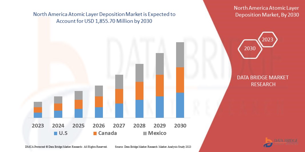
North America Atomic Layer Deposition Market Analysis and Size
Plastic recycling is process within which plastic wastes turn into useful products. Large production of non-biodegradable plastic across the globe is supporting plastic recycling to reduce soil pollution, water pollution, and air pollution which ultimately lowers carbon dioxide emissions and waste quantities.
Data Bridge Market Research analyses that the North America atomic layer deposition market which was USD 619.44 million in 2022, is expected to reach USD 1,855.70 million by 2030, and is expected to undergo a CAGR of 14.07% during the forecast period of 2023 to 2030. “Polyethylene terephthalate (PET) polyester segment” dominates the polymer type segment of the North America atomic layer deposition market part owing to its use in the production of high-quality fabrics and its ability to blend with other materials in order to enhance wrinkle-free and stain-resistant qualities. In addition to the insights on market scenarios such as market value, growth rate, segmentation, geographical coverage, and major players, the market reports curated by the Data Bridge Market Research also include in-depth expert analysis, geographically represented company-wise production and capacity, network layouts of distributors and partners, detailed and updated price trend analysis and deficit analysis of supply chain and demand.
North America Atomic Layer Deposition Market Scope and Segmentation
|
Report Metric |
Details |
|
Forecast Period |
2023 to 2030 |
|
Base Year |
2022 |
|
Historic Years |
2021 (Customizable to 2015-2020) |
|
Quantitative Units |
Revenue in USD Thousand, Volumes in Tons, Pricing in USD |
|
Segments Covered |
Product Type (Metal ALD, Aluminium Oxide ALD, Plasma Enhanced ALD, Catalytic ALD, Others), Application (Semiconductors, Solar Devices, Electronics, Medical Equipment, Research & Development Facilities, Fuel Cells, Optical Devices, Thermoelectric Materials, Magnetic Heads, Sensors, Barrier Layers, Primer Layers, Non—IC Application, Others) |
|
Countries Covered |
U.S., Canada and Mexico |
|
Market Players Covered |
ADEKA CORPORATION (Japan), AIXTRON (Germany), Applied Materials, Inc. (USA), ASM International (Netherlands), LAM RESEARCH CORPORATION (USA), Tokyo Electron Limited (Tokyo), Kurt J. Lesker Company (U.S.), and Veeco Instruments Inc. (USA) |
|
Market Opportunities |
|
Market Definition
Atomic layer deposition (ALD) refers to the process of deposition of precursor materials on substrates for improving or modifying properties such as chemical resistance, strength, and conductivity. The process is considered a sub-division of chemical vapor deposition (CVD) in atomic layer deposition. Most of the time, two chemicals are utilized for the reaction, generally called precursors.
North America Atomic Layer Deposition Market Dynamics
Drivers
- High Demand for Microelectronics and Consumer Electronics
Microelectronics is a process of manufacturing electronic components at the microscopic level. The microelectronics market is rapidly growing due to the demand for inexpensive and lightweight equipment. Microelectronics components include transistors, capacitors, diodes, resistors, inductors, and others. All these electronic components are used to manufacture mobile phones, laptops, electronic toys, and others.
- Raising Concern on Energy Harvesting Results in High Growth of Photovoltaic (PV) Cells
Photovoltaic (PV) is commonly called an energy harvesting technology, and the technology is used to convert solar energy into electric energy, which is electricity. The demand for photovoltaic cells has been increasing due to the relatively low price and wide range of applications such as solar traffic lights, solar power pumps, solar lamps, solar power calculators, and others.
Opportunity
- Trend of Miniaturization
Miniaturization is the process of manufacturing the smallest mechanical, electronic, and optical devices. In other words, it is a process of making electronic devices smaller. Miniaturization is in trend because everyone wants smaller, compacted, more portable devices. Now nanotechnology has the potential to transform the molecular beam into Nano-devices (functional). This is a big step toward miniaturization.
Restraints/Challenges
- Alternatives of Atomic Layer Deposition
The chemical vapor deposition process is widely used to produce high-quality, high-performance thin films. The chemical vapor deposition process is commonly used in the semiconductor industry. On the other hand, physical vapor deposition (PVD) is a method used to produce thin films and coatings with high temperature, high strength, excellent abrasion resistance, and others. Chemical vapor deposition and physical vapor deposition can be used as alternatives to atomic layer deposition due to the below advantages over atomic layer deposition.
- High Initial Investment Costs
Atomic layer deposition (ALD) is the deposition of precursor materials on substrates to improve/modify properties such as conductivity, chemical resistance, and strength. To provide ALD services, the provider has to buy equipment for the atomic layer deposition process, such as Cambridge NanoTech Fiji F200 Atomic Layer Deposition System, Open Load ALD System: OpAL, ALD 200L Series from Kurt J. Lesker Company, Cambridge NanoTech Savannah Series Atomic Layer Deposition System, Plasma & Thermal ALD System: FlexAL, Ion Beam Deposition System: IonFab IBD and Cambridge NanoTech Savannah Series Atomic Layer Deposition System.
North America Atomic Layer Deposition Market Scope
The North America atomic layer deposition market is segmented on the basis of product type and application. The growth amongst these segments will help you analyze meagre growth segments in the industries and provide the users with a valuable market overview and market insights to help them make strategic decisions for identifying core market applications.
Product Type
- Collection & transportation Metal ALD
- Aluminium Oxide ALD
- Plasma Enhanced ALD
- Catalytic ALD
- Others
Application
- Polyethylene Terephthalate Semiconductors
- Electronics
- Solar Devices
- Medical Equipment
- Optical Devices
- Thermoelectric Materials
- Fuel Cells
- Research & Development Facilities
- Magnetic Heads
- Sensors
- Barrier Layers
- Primer Layers
- Non-IC Application
- Others
North America Atomic Layer Deposition Market Regional Analysis/Insights
The North America atomic layer deposition market is analyzed, and market size insights and trends are provided based on country, product type and application as referenced above.
Some countries covered in the North America atomic layer deposition market report are the U.S., Canada, and Mexico.
The U.S. is expected to dominate the North America atomic layer deposition market in terms of market share and revenue. It is estimated to maintain its dominance during the forecast period due to the growing concerns about energy harvesting resulting in the high growth of photovoltaic (PV) cells.
The country section of the report also provides individual market impacting factors and changes in regulation in the market domestically that impacts the current and future trends of the market. Data points like down-stream and upstream value chain analysis, technical trends and porter's five forces analysis, case studies are some of the pointers used to forecast the market scenario for individual countries. Also, the presence and availability of global brands and their challenges faced due to large or scarce competition from local and domestic brands, impact of domestic tariffs and trade routes are considered while providing forecast analysis of the country data.
Competitive Landscape and North America Atomic Layer Deposition Market Share Analysis
The North America atomic layer deposition market competitive landscape provides details by competitor. Details included are company overview, company financials, revenue generated, market potential, investment in research and development, new market initiatives, global presence, production sites and facilities, production capacities, company strengths and weaknesses, product launch, product width and breadth, application dominance. The above data points provided are only related to the companies' focus related to North America atomic layer deposition market.
Some of the major players operating in the North America atomic layer deposition market are:
- ADEKA CORPORATION (Japan)
- AIXTRON (Germany)
- Applied Materials, Inc. (USA)
- ASM International (Netherlands)
- LAM RESEARCH CORPORATION (USA)
- Tokyo Electron Limited (Tokyo)
- Kurt J. Lesker Company (U.S.)
- Veeco Instruments Inc. (USA)
SKU-
- Interactive Data Analysis Dashboard
- Company Analysis Dashboard for high growth potential opportunities
- Research Analyst Access for customization & queries
- Competitor Analysis with Interactive dashboard
- Latest News, Updates & Trend analysis
- Harness the Power of Benchmark Analysis for Comprehensive Competitor Tracking
North America Atomic Layer Deposition Market, Supply Chain Analysis and Ecosystem Framework
To support market growth and help clients navigate the impact of geopolitical shifts, DBMR has integrated in-depth supply chain analysis into its North America Atomic Layer Deposition Market research reports. This addition empowers clients to respond effectively to global changes affecting their industries. The supply chain analysis section includes detailed insights such as North America Atomic Layer Deposition Market consumption and production by country, price trend analysis, the impact of tariffs and geopolitical developments, and import and export trends by country and HSN code. It also highlights major suppliers with data on production capacity and company profiles, as well as key importers and exporters. In addition to research, DBMR offers specialized supply chain consulting services backed by over a decade of experience, providing solutions like supplier discovery, supplier risk assessment, price trend analysis, impact evaluation of inflation and trade route changes, and comprehensive market trend analysis.
Data collection and base year analysis are done using data collection modules with large sample sizes. The stage includes obtaining market information or related data through various sources and strategies. It includes examining and planning all the data acquired from the past in advance. It likewise envelops the examination of information inconsistencies seen across different information sources. The market data is analysed and estimated using market statistical and coherent models. Also, market share analysis and key trend analysis are the major success factors in the market report. To know more, please request an analyst call or drop down your inquiry.
The key research methodology used by DBMR research team is data triangulation which involves data mining, analysis of the impact of data variables on the market and primary (industry expert) validation. Data models include Vendor Positioning Grid, Market Time Line Analysis, Market Overview and Guide, Company Positioning Grid, Patent Analysis, Pricing Analysis, Company Market Share Analysis, Standards of Measurement, Global versus Regional and Vendor Share Analysis. To know more about the research methodology, drop in an inquiry to speak to our industry experts.
Data Bridge Market Research is a leader in advanced formative research. We take pride in servicing our existing and new customers with data and analysis that match and suits their goal. The report can be customized to include price trend analysis of target brands understanding the market for additional countries (ask for the list of countries), clinical trial results data, literature review, refurbished market and product base analysis. Market analysis of target competitors can be analyzed from technology-based analysis to market portfolio strategies. We can add as many competitors that you require data about in the format and data style you are looking for. Our team of analysts can also provide you data in crude raw excel files pivot tables (Fact book) or can assist you in creating presentations from the data sets available in the report.


