Overview
Silicon wafers provide the foundation for the fabrication of many advanced semiconductor goods, which in turn create the foundation upon which the semiconductor industry is formed. A gradual change is witnessed in the size and diameter of silicon wafers over a few years. This ultimately leads to a new wave of discussions about going beyond the current wafer size majorly due to the increasing demand for advanced semiconductor goods, primarily as a means of enhancing the rate at which new semiconductor FABs and OSATs are produced. Currently, 200 mm (7.9/8 inch) wafers are the focus of most FABs and OSATs, with a small number concentrating on 300 mm (11.8/12 inch) wafers. In the end, wafer size selection is more investment and strategy-driven than technical. This is because every alteration in wafer size affects the entire end-to-end semiconductor flow.
The need for 200 mm capacity has been increasing owing to the development in demand for Internet of Things (IoT), mobile, and automotive applications. These applications are reviving 200 mm production and drive the need for components such as power, analogue, MEMS, and sensors. They do not necessitate cutting edge manufacturing processes. Different integrated Device Manufacturer (IDM) are moving to 8-inch wafer production for third-generation semiconductors including GaN and SiC.
Impact of Wafer Size on Semiconductor Industry
A key factor in determining the construction of the FABs and OSATs is wafer size. The main cause is that the tools and equipment needed depend on the size of the wafer, and as wafer size increases, so does the expense of building up additional FABs and OSATs. For this reason, choosing the appropriate wafer size is essential. Wafer size selection is ultimately more strategy and investment-driven than technical. This is since every change in wafer size affects the semiconductor flow from beginning to finish.
Below points unequivocally demonstrate how wafer size affects several aspects of the semiconductor process. There are a number of factors to take into account when determining which wafer size will be utilized to create the next-generation product, ranging from cost to yield.
Figure 1: Factors Considered While Determining Wafer Sizes
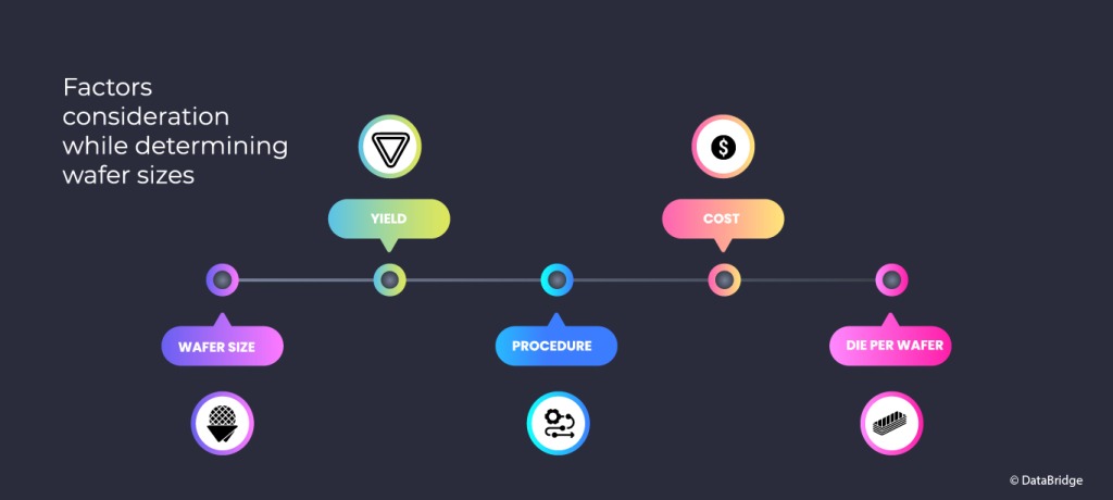
Wafer Size: More die per unit area is undoubtedly provided by larger wafer sizes. The greater area to create more die eventually allows FABs and OSATs to fabricate and test/assemble more dies in a given period. This accelerates the rate at which new products can be manufactured or assembled, and it may also benefit the supply chain in some cases when wafer size is increased.
Die Per Wafer: The number of die per wafer is directly related to wafer size as it makes possible for semiconductor design houses to estimate the amount of cost reduction. In the end, as compared to a bigger size wafer, a smaller wafer for a highly demanded product will result in the maximization of more wafer orders. Thus, companies frequently need to invest more time in weighing the benefits and drawbacks of using wafers from a commercial standpoint because of this delicate balancing act.
Procedure: As wafer size is considered to be the most important parameter, thus semiconductor manufacturing facilities must plan and determine in advance which wafer sizes they will support for the next five to ten years. The primary consideration is the expense of setting up the process necessary for every wafer size upgrade. Most semiconductor facilities have focused on 200 mm (7.9/8 inch) wafers since they allow for the balance of both the technical and business aspects. However the requirement for 300 mm (11.8/12 inch) is forcing FABs and OSATs to modernize.
Cost: The cost factor is also considered to be one of the most important factors for developing a semiconductor product as it is dominated by wafer size. In addition to the wafer's cost, FAB and OSAT expenses must be taken into account. When compared to a 300 mm (11.8/12 inch) wafer, the cost of producing and assembling semiconductor chips will undoubtedly be lower when using a 200 mm (7.9/8 inch) wafer. Ultimately, the key is to create the margin by choosing the appropriate wafer size.
Yield: Historically, yield has decreased as wafer size has increased. When a product is manufactured on a 200 mm (7.9/8 inch) wafer as opposed to a 300 mm (11.8/12 inch) wafer, the yield of the former will be lower. The final yield will ultimately be comparable, but as wafer sizes increase, yield will decrease mostly because it takes longer to perfect the semiconductor process. This process improves as more products use the same wafer size because lessons learned may be applied to boost total product yield. The final yield is also greatly influenced by wafer handling, and as wafer size increases, it becomes more challenging to reduce the number of process steps because of the significant number of die per given area.
The semiconductor manufacturing equipment market has witnessed a substantial growth owing to the growing demand for semiconductor parts in electric and hybrid vehicle. Adding to this, increase in manufacturing units for FABs construction supplements the growth in forecast period. According to Data Bridge Market Research analysis, the market for global semiconductor manufacturing equipment market is projected to grow at a compound annual growth rate (CAGR) of 9.5% from 2022- 2030.
To learn more about the study, visit: https://www.databridgemarketresearch.com/reports/global-semiconductor-manufacturing-equipment-market
Highlight towards the Chips Usage in Different Applications
According to SEMI, as the industry approaches a high record of more than 7.7 million wafers per month (wpm), semiconductor manufacturers globally are expected to increase 200mm fab capacity by 14% from 2023 through 2026, adding 12 new 200mm volume FABs (excluding EPI).
The primary drivers of 200 mm investment are power and compound semiconductors, which are essential to the automotive, industrial, and consumer sectors. As EV usage rises, it is anticipated that developments in powertrain inverters and EV charging stations, in particular, will drive increases in 200 mm wafer capacity globally. The rising chip content in EVs and the desire to shorten charging times are driving capacity expansions even while the supply of automotive chips has stabilized.
To fulfill future demand, chip providers such as STMicroelectronics, Bosch, Fuji Electric, Infineon, Mitsubishi, Onsemi, Rohm, and Wolfspeed are speeding up their 200mm capacity projects.
Global SiC power semiconductor market is witnessing a substantial growth in recent years owing to the rising demand for power electronics across various industries such as consumer electronics, automotive and industrial in developing countries is one of the factors. This is majorly due to is several advantages including compact design, simplified circuit, ability to withstand high current and voltage. According to Data Bridge Market Research analysis, the market for global SiC power semiconductor market is projected to grow at a compound annual growth rate (CAGR) of 9.5% from 2022- 2030.
To learn more about the study, visit: https://www.databridgemarketresearch.com/reports/global-sic-power-semiconductor-market
Fabricators have a strong incentive to shorten lead times given the strong demand for automobiles. The mature FABs that produce six- and eight-inch wafers, are mostly used in different automobile electronic control units, may find that challenging. These wafers are often older and less efficient. Production timeframes can be shortened by increasing automation and increasing production through new facilities and tool setup, but even in modern facilities, these strategies are difficult and time-consuming to adopt. Mature factories can adopt a more rigorous, all-encompassing strategy that concentrates on four essential tasks to increase production more quickly: enhancing overall equipment efficiency (OEE), controlling labor proactively, derisking infrastructure, and dynamically managing performance.
According to the SEMI 200mm Fab Outlook to 2026 report, fab capacity for power and automotive semiconductors will increase by 34% between 2023 and 2026. MEMS, Analogue, and Foundry will come in third and fourth, at 8%, 6%, and 8%, respectively, behind Microprocessor Unit/Microcontroller Unit (MPU/MCU), at 21%.
Regional Insights
During the peak of the COVID-19 epidemic in 2021, the U.S. experienced an abrupt and severe semiconductor shortage. Numerous significant businesses were badly impacted by this shortfall, including consumer electronics, household appliances, renewable energy, and automobiles. The shortfall had severe financial ramifications; the U.S. Department of Commerce estimates that it reduced U.S. economic growth by almost a quarter of a trillion dollars that year.
Beyond the financial ramifications, the chip shortage exposed the extent to which numerous U.S. businesses had become reliant on semiconductors made in Asia. The epidemic was an unpleasant awakening, a sharp shock. Due to the country's extensive reliance on semiconductors made in Asia, the economy was susceptible to unforeseen events.
The Creating Helpful Incentives to Produce Semiconductors and Science Act (CHIPS Act) was created as a result of the financial impact. The CHIPS and Science Act, which was signed into law on August 9, 2022, allocates around USD 53 billion to the advancement of "American semiconductor research, development, manufacturing, and workforce development," as stated in a news statement from the White House at the time.
A similar strategy was revealed by the European Union in April of 2023. The European Chips Act specifically aims to double the semiconductor industry's global market share from 10% to 20% by 2030 by allocating 43 billion euros, or approximately USD 47 billion, to the 27 member states.
In an attempt to gain more independence in semiconductor manufacture, Europe and the US are currently launching massive construction projects to construct their own semiconductor fabrication facilities.
For instance,
In order to make economies more resilient to future geopolitical crises, the U.S. and European countries are strengthening their supply chains and boosting the amount of chips manufactured domestically.
Figure 2: 200 mm Equivalent New Capacity, By Region, (2022-2025)
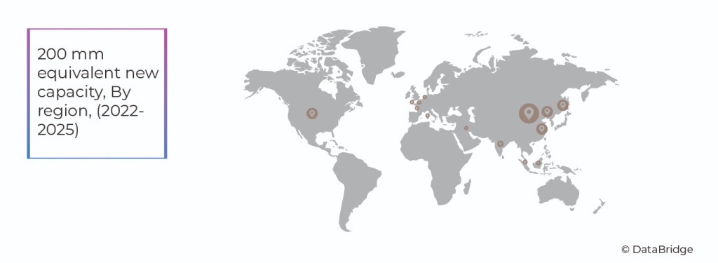
Source: DBMR analysis
According to Data Bridge Market Research analysis, Asia-Pacific region holds a major share in 200mm & 300 mm fab capacity, as compared to other regions namely Europe & Mideast, and America. This is majorly due to advanced infrastructure, significant presence of market players, robust investment in research and development, and stringent government initiatives towards adoption among others. Moreover, Asia-Pacific region is considered to be the biggest semiconductor market with countries including China, Taiwan, and Japan.
Figure 3: Estimated Market Share for 200 mm New Production Capacity, By Region, (2022-2025)
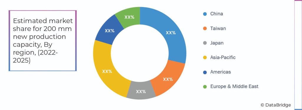
Source: DBMR analysis
Regarding manufacturing, China continues to be the front-runner when it comes to investments for 300mm as well as 200 and 150mm production expansion. Main power IDMs are building new 300mm lines, or expanding existing ones. The ecosystem includes companies such as Bosch, Toshiba, Infineon Technologies, and Nexperia. There are a few 200mm lines being constructed globally, and 150mm lines are being converted to 200mm. Aside from that, power IDMs vying for 200mm SiC capacity include Wolfspeed, Infineon Technologies, CRCC, and others.
Initiatives Taken by Different Manufacturers Towards Increase in the Production Capacity
Below are few of the strategic initiatives taken by different manufacturers to increase the production capacity:
Global electric vehicle market is witnessing a significant growth in recent years due to several factors such as increasing government initiatives towards electric vehicles (EVs), reduction in the EV battery prices, development of public and private electric vehicle charging, advancement of EV charging technologies via wireless means and lots more. According to Data Bridge Market Research analysis, the market for global electric vehicle market is projected to grow at a compound annual growth rate (CAGR) of 20.35% from 2023- 2030.
To learn more about the study, visit: https://www.databridgemarketresearch.com/reports/global-electric-vehicle-market
Recommendations for Semiconductor Industry in Future Towards a New Wafer Size
The ongoing crisis of semiconductor scarcity is also prompting discussions about expanding the setup and pursuing the largest wafer size currently being produced, 300 mm (11.8/12 inch).
This entails requiring all future FABs and OSAT designs to choose 300 mm or even 450 mm (17.7/18 inch), which have not yet been employed for full-scale manufacture. The main point of contention is that by giving FABs and OSATs the means to produce more dies per unit space, they may enhance their capacity. A significant expenditure will undoubtedly be needed for this, and few FAB/OSAT will choose a wafer larger than 200 mm (7.9/8 inch).
Wafer size is another factor that the semiconductor industry should consider given the increasing reliance on semiconductor devices. Building more FABs and OSATs and outfitting them for future requirements is the most effective strategy to remove any future demand that causes the shortage. The FABs/OSATs should begin planning for 450 mm now even if they are first constructed and equipped with a 200 mm or 300 mm wafer. By adopting such a plan, FABs and OSATs will be prepared for future demand, which may undoubtedly surpass the total capacity that will be accessible in the near future.
Strong measures are needed to encourage the use of wafer sizes that are significantly larger than those now manufactured, primarily 450 mm. The roadmap below offers a comprehensive explanation of the reasons why distinct actions should be made in the direction of larger wafer sizes.
Capacity: Given the scarcity of semiconductors, today's capacity—which is based on a variety of wafer sizes—is undoubtedly insufficient. Increasing the number of FABs and OSATs will undoubtedly boost capacity, but not as much as increasing the wafer size. The companies that produce semiconductors must consider the long-term costs of holding off on upgrading to larger wafer sizes. Wafer FABs/OSATs in the 300 mm range can be the starting point, and it can go to 450 mm.
FAB-LITE: Developing a few specialized semiconductor FABs and OSATs that exclusively serve future huge wafer sizes is another strategy for managing wafer size. These could be facilities dedicated to wafer FABs/OSATs with dimensions of 450 or 675 mm (26.6/27 inch). According to this plan, the new buildings will serve as research and development hubs for larger wafer sizes in the future. As technology advances, mass manufacturing will be made possible by the decreased cost of using these larger wafer sizes.
Cooperation: It is expensive to set up FABs and OSATs that can process higher wafer sizes. Bringing together various manufacturers and investing in cluster-based facilities that serve various clientele is the only option to reduce this expense. While IP and other confidential issues will undoubtedly arise from this, capacity focused on larger wafer sizes cannot be increased without cooperation.
Target Node: For particular technology nodes, larger wafer sizes may also be employed. In this approach, the necessary investment and the cost of manufacturing can both be balanced. Older nodes with more reliable processes than those with upcoming new technologies may be the most appropriate nodes. This can undoubtedly encourage the use of larger wafer sizes as well.
Efficiency: Ultimately, by shipping more parts in the same amount of time, higher wafer sizes improve efficiency. As long as the production technology is economical, the total cost and investment will equalize. This is just another argument in favor of bigger wafer sizes in the semiconductor industry.
Conclusion
Lack of 8-inch wafer production capacity is mostly due to the ongoing rise in demand for these mixed signal processors and power devices. It would seem that foundries would be expanding their capacity since the supply of 8-inch wafers is at an all-time high. Furthermore, foundries are interested in purchasing 8-inch production lines and related machinery from IDMs. It has been witnessed that very few suppliers are currently producing 8-inch semiconductor equipment, which means the price of such equipment has suddenly risen, there has been a serious scarcity since 2019. This has resulted that some foundries have increased the price for 8-inch wafers to their customers.
It has been witnessed that certain IC producers are transferring their current designs from 8-inch lines with 180 nm and 350 nm to newer lines with 12-inch wafers. Additionally, a large number of foundries provide appropriate 130 nm processes produced on 12-inch wafers, which can be employed as a backup or primary source to meet future capacity requirements and diversify the supply chain geographically.
Organizations who currently use silicon on 8-inch wafers should priorities an evaluation of their future needs, as the current shortages should be interpreted as a warning. If a substantial amount of capacity is needed, they ought to think about migrating to a 12-inch node and give themselves the time to finish the process at either the primary or secondary source production plant
DBMR has served more than 40% of Fortune 500 firms internationally and has a network of more than 5000 clients. Our Team would be happy to help you with your queries. Visit, https://www.databridgemarketresearch.com/contact
Contact Us