
Global Mask Alignment System Market
Market Size in USD Billion
 USD
1.50 Billion
USD
3.05 Billion
2024
2032
USD
1.50 Billion
USD
3.05 Billion
2024
2032
| 2025 - 2032 | |
| USD 1.50 Billion | |
| USD 3.05 Billion | |
| % | |
|
Mask Alignment System Market Analysis
The mask alignment system market is witnessing significant growth driven by advancements in semiconductor manufacturing technologies. Mask alignment systems play a crucial role in photolithography, ensuring precise alignment of the mask with the wafer during the patterning process. This precision is critical for the production of smaller and more complex integrated circuits. The market is seeing continuous improvements in system accuracy, speed, and automation, helping meet the growing demand for smaller, faster, and more efficient electronic devices. One of the key advancements is the development of high-NA (Numerical Aperture) mask alignment systems, which provide higher resolution and better alignment accuracy, making them suitable for next-generation semiconductor devices. In addition, the integration of automated systems has streamlined production processes, reducing human error and increasing throughput in semiconductor fabs. Companies such as ASML, EV Group, and Canon are leading the market with their innovative solutions, such as multi-beam and laser-based systems, which enhance alignment precision and speed.
The shift towards advanced semiconductor technologies, such as 5G, AI, and IoT, is driving the demand for more sophisticated mask alignment systems. These advancements are expected to further accelerate the growth of the market as industries continue to push the boundaries of electronics manufacturing.
Mask Alignment System Market Size
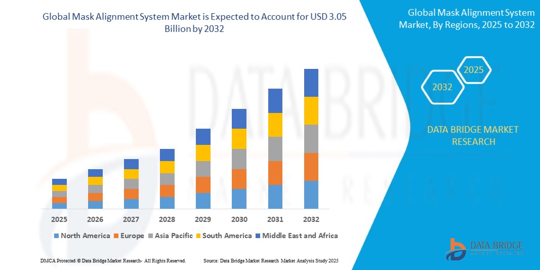
The global mask alignment system market size was valued at USD 1.50 billion in 2024 and is projected to reach USD 3.05 billion by 2032, with a CAGR of 9.30% during the forecast period of 2025 to 2032. In addition to the insights on market scenarios such as market value, growth rate, segmentation, geographical coverage, and major players, the market reports curated by the Data Bridge Market Research also include in-depth expert analysis, geographically represented company-wise production and capacity, network layouts of distributors and partners, detailed and updated price trend analysis and deficit analysis of supply chain and demand.
Mask Alignment System Market Trends
“Increasing Shift towards Automation and High-Precision Technologies”
One of the prominent trends in the mask alignment system market is the increasing shift towards automation and high-precision technologies to meet the demands of next-generation semiconductor manufacturing. As the industry moves towards smaller nodes, particularly in the production of advanced microchips for applications such as AI, 5G, and IoT, the need for higher alignment accuracy and throughput is paramount. For instance, high-NA (Numerical Aperture) lithography systems from companies such as ASML and Canon are enhancing the resolution and precision of patterning, which is crucial for advanced semiconductor fabrication. In addition, automation in mask alignment systems is streamlining the production process, reducing human errors, and increasing overall efficiency. Automated systems enable faster throughput and more consistent results, making them ideal for large-scale semiconductor fabrication. This trend is expected to drive further growth in the Mask Alignment System market as the demand for more sophisticated, efficient, and high-precision manufacturing solutions continues to rise across the global electronics sector.
Report Scope and Mask Alignment System Market Segmentation
|
Attributes |
Mask Alignment System Key Market Insights |
|
Segments Covered |
|
|
Countries Covered |
U.S., Canada and Mexico in North America, Germany, France, U.K., Netherlands, Switzerland, Belgium, Russia, Italy, Spain, Turkey, Rest of Europe in Europe, China, Japan, India, South Korea, Singapore, Malaysia, Australia, Thailand, Indonesia, Philippines, Rest of Asia-Pacific (APAC) in the Asia-Pacific (APAC), Saudi Arabia, U.A.E., South Africa, Egypt, Israel, Rest of Middle East and Africa (MEA) as a part of Middle East and Africa (MEA), Brazil, Argentina and Rest of South America as part of South America |
|
Key Market Players |
EV Group (EVG) (Austria), SUSS MicroTec SE (Germany), Canon Inc. (Japan), Nikon Corporation (Japan), ASML (Netherlands), Ultratech Inc. (U.S.), Neutronix Inc. (U.S.), OAI (Optical Associates, Inc.) (U.S.), Veeco Instruments Inc. (U.S.), HTG, Inc. (U.S.), MicroTec GmbH (Germany), JENOPTIK AG (Germany), Onto Innovation (U.S.), Applied Materials, Inc. (U.S.), Tokyo Electron Limited (Japan), KLA Corporation (U.S.), DISCO Corporation (Japan), Vistec Electron Beam GmbH (Germany), Bruker (U.S.), Aixtron (Germany), Ushio America, Inc. (U.S.), and Attocube Systems AG (Germany). |
|
Market Opportunities |
|
|
Value Added Data Infosets |
In addition to the insights on market scenarios such as market value, growth rate, segmentation, geographical coverage, and major players, the market reports curated by the Data Bridge Market Research also include in-depth expert analysis, geographically represented company-wise production and capacity, network layouts of distributors and partners, detailed and updated price trend analysis and deficit analysis of supply chain and demand. |
Mask Alignment System Market Definition
A Mask Alignment System is a crucial tool in semiconductor manufacturing used to align photomasks with substrates, such as silicon wafers, during the photolithography process. This system ensures that precise patterns on the mask are accurately transferred onto the wafer’s surface, allowing for the fabrication of microelectronic components such as integrated circuits.
Mask Alignment System Market Dynamics
Drivers
- Growth in Semiconductor Industry
The global demand for electronic devices, such as smartphones, laptops, and high-performance computing systems, has seen a significant rise over recent years. This surge in demand is directly linked to the rapid development of the semiconductor industry. With the need for increasingly powerful microchips that support AI, 5G, autonomous vehicles, and data centers, semiconductor manufacturers are focusing on miniaturizing and optimizing chip designs. As a result, advanced semiconductor production techniques, such as extreme ultraviolet (EUV) lithography, require the use of precise mask alignment systems. These systems are essential to ensure the accurate transfer of microscopic patterns onto semiconductor wafers, crucial for producing next-generation chips. The growing demand for smaller, faster, and more energy-efficient semiconductors drives the need for higher alignment precision, positioning mask alignment systems as a key factor in this manufacturing process. For instance, companies such as ASML and Nikon are developing more advanced lithography and alignment tools to meet the challenges posed by ever-decreasing node sizes in semiconductor fabrication.
- Rising Demand for Consumer Electronics and IoT Devices
The ever-expanding market for consumer electronics, including smartphones, smart wearables, and IoT devices, has increased the demand for semiconductors capable of powering these devices. These devices require increasingly sophisticated chip designs to support connectivity, processing power, and efficient performance. As a result, manufacturers are incorporating advanced semiconductor technologies into these consumer products. Mask alignment systems play a crucial role in ensuring the production of high-quality microchips by accurately transferring patterns onto wafers. For instance, in the production of microprocessors for smartphones or memory chips for IoT devices, precise alignment is needed to ensure the functionality of these components. As consumer demand continues to rise for cutting-edge electronics, the need for improved manufacturing processes, including the use of mask alignment systems, becomes even more critical. Companies such as Intel and Qualcomm are leveraging these systems to produce the microchips that power everything from wearable fitness trackers to connected home devices, pushing the market for alignment systems even further.
Opportunities
- Increasing Advancements in Lithography Technology
The semiconductor industry is constantly evolving, with manufacturers pushing for smaller node sizes and more powerful chips. To achieve these advancements, cutting-edge photolithography techniques such as extreme ultraviolet (EUV) lithography and multi-patterning have become essential. These innovations allow for the fabrication of smaller, more complex semiconductor devices. However, as semiconductor nodes shrink to 5nm and below, the need for highly precise alignment systems becomes increasingly crucial. Mask alignment systems are directly linked to these advancements, as they ensure that the intricate patterns required for modern chips are precisely transferred onto wafers without any misalignment or defects. For instance, ASML's EUV lithography systems are driving the shift toward smaller node sizes, but these systems require highly accurate mask aligners to support their functionality. As semiconductor manufacturers aim to achieve ever-smaller and more complex nodes, mask alignment systems that can meet stringent alignment specifications will continue to see significant demand, positioning them as a key market opportunity.
- Increasing Focus on Advanced Packaging
The rising demand for heterogeneous integration and advanced packaging techniques is reshaping the semiconductor landscape, driving a need for more sophisticated manufacturing tools. Advanced packaging, such as 3D stacking and system-in-package (SiP), involves stacking multiple chips or integrating various semiconductor components into a single package. These technologies enable improved performance, reduced size, and lower power consumption, making them critical for applications such as high-performance computing, smartphones, and IoT devices. However, the alignment of complex patterns on stacked wafers or multi-chip packages requires precise mask alignment systems to ensure that each layer of the chip is correctly positioned. For instance, in the production of 3D NAND flash memory or high-bandwidth memory, precise alignment is necessary to maintain chip integrity and functionality. As the adoption of advanced packaging techniques continues to grow, the need for advanced mask alignment systems capable of handling these complex processes presents a significant market opportunity. The demand for these systems is being fueled by companies such as TSMC, Samsung, and Intel, which are investing heavily in advanced packaging to remain competitive in the rapidly evolving semiconductor market.
Restraints/Challenges
- High Cost of Equipment
One of the major challenges facing the mask alignment system market is the high cost of equipment. Mask alignment systems are complex and require advanced technology to provide the precision necessary for semiconductor manufacturing. These systems are typically high-investment, both in terms of the initial purchase price and the maintenance required to keep them functioning at peak performance. For smaller manufacturers or startups, the high costs associated with acquiring and maintaining these systems can be a significant barrier to entry. For instance, the cost of installing an extreme ultraviolet (EUV) lithography machine, which relies on high-precision alignment systems, can exceed several million dollars. As a result, the high capital expenditure needed to invest in these systems may limit the adoption of mask alignment systems, especially in emerging markets or by companies with smaller production scales. This challenge could slow market growth, as businesses must balance precision needs with financial constraints.
- Shortage of Skilled Workforce
As the mask alignment system market continues to evolve with more complex technology, the need for a highly skilled workforce becomes more pressing. Operating and maintaining precision mask alignment equipment requires technical expertise in areas such as optics, lithography, and semiconductor manufacturing processes. However, the semiconductor industry is experiencing a shortage of skilled workers in these highly specialized fields. This talent gap can hinder manufacturers' ability to fully leverage mask alignment systems, potentially impacting productivity and system reliability. For instance, trained engineers are required to ensure the alignment systems operate correctly and maintain their precision throughout the production process. The shortage of qualified professionals poses a significant challenge to the market, as it affects both the development and maintenance of the equipment. To address this, companies may need to invest in training programs and upskilling initiatives, which adds to operational costs and could slow the adoption of newer, more complex alignment technologies.
This market report provides details of new recent developments, trade regulations, import-export analysis, production analysis, value chain optimization, market share, impact of domestic and localized market players, analyses opportunities in terms of emerging revenue pockets, changes in market regulations, strategic market growth analysis, market size, category market growths, application niches and dominance, product approvals, product launches, geographic expansions, technological innovations in the market. To gain more info on the market contact Data Bridge Market Research for an Analyst Brief, our team will help you take an informed market decision to achieve market growth.
Mask Alignment System Market Scope
The market is segmented on the basis of type, applications, and end-user. The growth amongst these segments will help you analyse meagre growth segments in the industries and provide the users with a valuable market overview and market insights to help them make strategic decisions for identifying core market applications.
Type
- Semi-Automated
- Fully Automated
Application
- MEMS Devices
- Compound Semiconductor
- LED Devices
End-User
- Foundry/Factory
- Memory Chips Manufacturers
- IDM (Integrated Device Manufacturer)
Mask Alignment System Market Regional Analysis
The market is analysed and market size insights and trends are provided by country, type, applications, and end-user as referenced above.
The countries covered in the market report are U.S., Canada and Mexico in North America, Germany, France, U.K., Netherlands, Switzerland, Belgium, Russia, Italy, Spain, Turkey, Rest of Europe in Europe, China, Japan, India, South Korea, Singapore, Malaysia, Australia, Thailand, Indonesia, Philippines, Rest of Asia-Pacific (APAC) in the Asia-Pacific (APAC), Saudi Arabia, U.A.E., South Africa, Egypt, Israel, Rest of Middle East and Africa (MEA) as a part of Middle East and Africa (MEA), Brazil, Argentina and Rest of South America as part of South America.
Asia-Pacific is dominating the global mask alignment system market due to the rapid growth of semiconductor and electronics industries in the region. The increasing demand for advanced semiconductor devices, particularly in countries such as China, Japan, and South Korea, is driving the need for precise alignment systems. In addition, the presence of major semiconductor manufacturing companies and a growing number of research and development facilities in the region further contribute to its dominance. This market trend is expected to continue as Asia-Pacific remains the hub for semiconductor innovation and production.
The country section of the report also provides individual market impacting factors and changes in regulation in the market domestically that impacts the current and future trends of the market. Data points such as down-stream and upstream value chain analysis, technical trends and porter's five forces analysis, case studies are some of the pointers used to forecast the market scenario for individual countries. Also, the presence and availability of global brands and their challenges faced due to large or scarce competition from local and domestic brands, impact of domestic tariffs and trade routes are considered while providing forecast analysis of the country data.
Mask Alignment System Market Share
The market competitive landscape provides details by competitor. Details included are company overview, company financials, revenue generated, market potential, investment in research and development, new market initiatives, global presence, production sites and facilities, production capacities, company strengths and weaknesses, product launch, product width and breadth, application dominance. The above data points provided are only related to the companies' focus related to market.
Mask Alignment System Market Leaders Operating in the Market Are:
- EV Group (EVG) (Austria)
- SUSS MicroTec SE (Germany)
- Canon Inc. (Japan)
- Nikon Corporation (Japan)
- ASML (Netherlands)
- Ultratech Inc. (U.S.)
- Neutronix Inc. (U.S.)
- OAI (Optical Associates, Inc.) (U.S.)
- Veeco Instruments Inc. (U.S.)
- HTG, Inc. (U.S.)
- MicroTec GmbH (Germany)
- JENOPTIK AG (Germany)
- Onto Innovation (U.S.)
- Applied Materials, Inc. (U.S.)
- Tokyo Electron Limited (Japan)
- KLA Corporation (U.S.)
- DISCO Corporation (Japan)
- Vistec Electron Beam GmbH (Germany)
- Bruker (U.S.)
- Aixtron (Germany)
- Ushio America, Inc. (U.S.)
- Attocube Systems AG (Germany)
Latest Developments in Mask Alignment System Market
- In June 2024, Multibeam Corp. introduced its MB platform, the first-ever Multicolumn E-Beam Lithography (MEBL) system, designed to improve chip manufacturing. This fully automated, precision-patterning technology is intended for mass production, with applications in rapid prototyping, advanced packaging, high-mix production, chip identification, compound semiconductors, and more
- In January 2024, ZEISS, in collaboration with ASML Holding, launched high NA-EUV lithography technology, which will enable a threefold increase in transistor density for advanced microchips. This breakthrough European technology, featuring ZEISS's ultra-precise optical system developed over 25 years, is set to power the first series production of next-generation microchips in 2025
- In October 2023, Canon released the FPA-1200NZ2C nanoimprint semiconductor manufacturing equipment, designed to carry out circuit pattern transfers, an essential step in semiconductor production
- In December 2022, Bruker Corporation acquired Neurescence Inc., a leading developer of ultralight fiber-bundle Multiscopes™ for optical functional neuroimaging in multi-regions. This acquisition strengthens Bruker's position in the field of freely behaving animal imaging and photostimulation, expanding their research and imaging capabilities for emerging trends
- In July 2021, Qualcomm partnered with General Motors to incorporate AI and 5G connectivity into future automotive systems. This collaboration aims to develop next-generation telematics systems and enhance the performance of ADAS and autonomous driving by powering digital cockpits
SKU-
- Interactive Data Analysis Dashboard
- Company Analysis Dashboard for high growth potential opportunities
- Research Analyst Access for customization & queries
- Competitor Analysis with Interactive dashboard
- Latest News, Updates & Trend analysis
- Harness the Power of Benchmark Analysis for Comprehensive Competitor Tracking
Global Mask Alignment System Market, Supply Chain Analysis and Ecosystem Framework
To support market growth and help clients navigate the impact of geopolitical shifts, DBMR has integrated in-depth supply chain analysis into its Global Mask Alignment System Market research reports. This addition empowers clients to respond effectively to global changes affecting their industries. The supply chain analysis section includes detailed insights such as Global Mask Alignment System Market consumption and production by country, price trend analysis, the impact of tariffs and geopolitical developments, and import and export trends by country and HSN code. It also highlights major suppliers with data on production capacity and company profiles, as well as key importers and exporters. In addition to research, DBMR offers specialized supply chain consulting services backed by over a decade of experience, providing solutions like supplier discovery, supplier risk assessment, price trend analysis, impact evaluation of inflation and trade route changes, and comprehensive market trend analysis.
Data collection and base year analysis are done using data collection modules with large sample sizes. The stage includes obtaining market information or related data through various sources and strategies. It includes examining and planning all the data acquired from the past in advance. It likewise envelops the examination of information inconsistencies seen across different information sources. The market data is analysed and estimated using market statistical and coherent models. Also, market share analysis and key trend analysis are the major success factors in the market report. To know more, please request an analyst call or drop down your inquiry.
The key research methodology used by DBMR research team is data triangulation which involves data mining, analysis of the impact of data variables on the market and primary (industry expert) validation. Data models include Vendor Positioning Grid, Market Time Line Analysis, Market Overview and Guide, Company Positioning Grid, Patent Analysis, Pricing Analysis, Company Market Share Analysis, Standards of Measurement, Global versus Regional and Vendor Share Analysis. To know more about the research methodology, drop in an inquiry to speak to our industry experts.
Data Bridge Market Research is a leader in advanced formative research. We take pride in servicing our existing and new customers with data and analysis that match and suits their goal. The report can be customized to include price trend analysis of target brands understanding the market for additional countries (ask for the list of countries), clinical trial results data, literature review, refurbished market and product base analysis. Market analysis of target competitors can be analyzed from technology-based analysis to market portfolio strategies. We can add as many competitors that you require data about in the format and data style you are looking for. Our team of analysts can also provide you data in crude raw excel files pivot tables (Fact book) or can assist you in creating presentations from the data sets available in the report.


